Altera Arria V Avalon-ST User Manual
Page 188
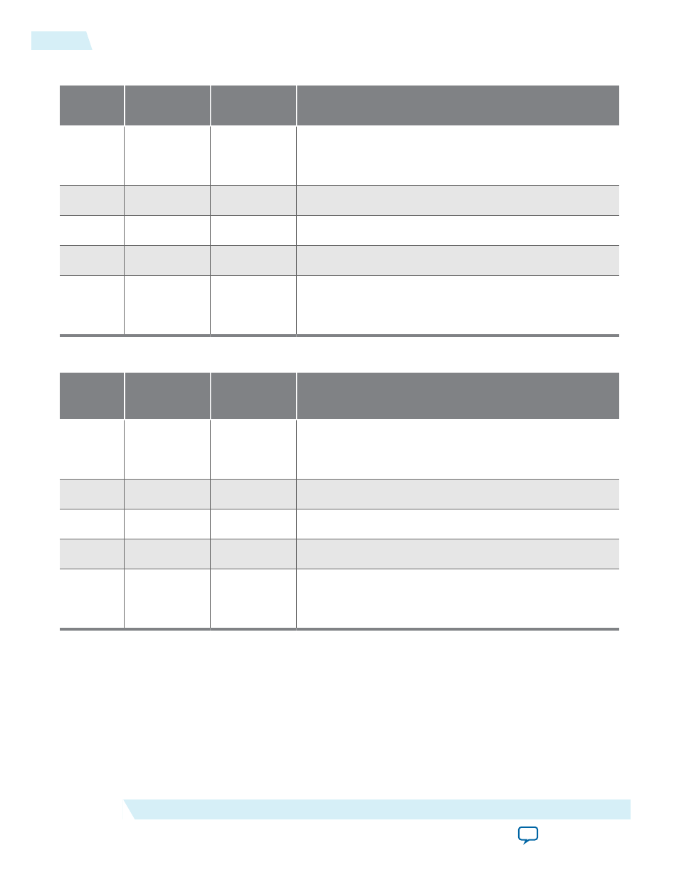
Table 16-12: Write Descriptor 1
Offset in BFM
Shared Memory
Value
Description
DW0
0x820
1,024
Transfer length in dwords and control bits as described in
Bit Definitions for the Control Field in the DMA Write
Control Register and DMA Read Control Register .
DW1
0x824
0
Endpoint address
DW2
0x828
0
BFM shared memory data buffer 1 upper address value
DW3
0x82c
0x2800
BFM shared memory data buffer 1 lower address value
Data
Buffer 1
0x02800
Increment by 1
from 0x2525_
0001
Data content in the BFM shared memory from address:
0x02800
Table 16-13: Write Descriptor 2
Offset in BFM
Shared Memory
Value
Description
DW0
0x830
644
Transfer length in dwords and control bits as described in
Bit Definitions for the Control Field in the DMA Write
Control Register and DMA Read Control Register.
DW1
0x834
0
Endpoint address
DW2
0x838
0
BFM shared memory data buffer 2 upper address value
DW3
0x83c
0x057A0
BFM shared memory data buffer 2 lower address value
Data
Buffer 2
0x057A0
Increment by 1
from 0x3535_
0001
Data content in the BFM shared memory from address:
0x057A0
2. Sets up the chaining DMA descriptor header and starts the transfer data from the Endpoint memory to
the BFM shared memory. The transfer calls the procedure
dma_set_header
which writes four dwords,
DW0:DW3, into the DMA write register module.
16-18
DMA Write Cycles
2014.12.15
Altera Corporation
Testbench and Design Example