Endpoint testbench – Altera Arria V Avalon-ST User Manual
Page 172
Your Application Layer design may need to handle at least the following scenarios that are not possible to
create with the Altera testbench and the Root Port BFM:
• It is unable to generate or receive Vendor Defined Messages. Some systems generate Vendor Defined
Messages and the Application Layer must be designed to process them. The Hard IP block passes these
messages on to the Application Layer which, in most cases should ignore them.
• It can only handle received read requests that are less than or equal to the currently set Maximum
payload size option specified under PCI Express/PCI Capabilities heading under the Device tab
using the parameter editor. Many systems are capable of handling larger read requests that are then
returned in multiple completions.
• It always returns a single completion for every read request. Some systems split completions on every
64-byte address boundary.
• It always returns completions in the same order the read requests were issued. Some systems generate
the completions out-of-order.
• It is unable to generate zero-length read requests that some systems generate as flush requests
following some write transactions. The Application Layer must be capable of generating the
completions to the zero length read requests.
• It uses fixed credit allocation.
• It does not support parity.
• It does not support multi-function designs which are available when using Configuration Space Bypass
mode or Single Root I/O Virtualization (SR-IOV).
Endpoint Testbench
After you install the Quartus II software, you can copy any of the example designs from the
<install_dir>/ip/
altera/altera_pcie/altera_pcie_hip_ast_ed/example_design
directory. You can generate the testbench from the
example design as was shown in Getting Started with the Arria V Hard IP for PCI Express.
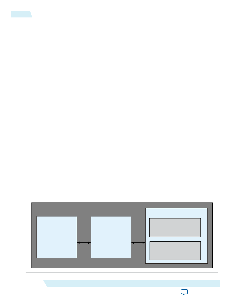
This testbench simulates up to an ×8 PCI Express link using either the PIPE interfaces of the Root Port
and Endpoints or the serial PCI Express interface. The testbench design does not allow more than one
PCI Express link to be simulated at a time. The following figure presents a high level view of the design
example.
Figure 16-1: Design Example for Endpoint Designs
APPS
altpcied_<dev>_hwtcl.v
Hard IP for PCI Express Testbench for Endpoints
Avalon-ST TX
Avalon-ST RX
reset
status
Avalon-ST TX
Avalon-ST RX
reset
status
DUT
altpcie_<dev>_hip_ast_hwtcl.v
Root Port Model
altpcie_tbed_<dev>_hwtcl.v
PIPE or
Serial
Interface
Root Port BFM
altpcietb_bfm_rpvar_64b_x8_pipen1b
Root Port Driver and Monitor
altpcietb_bfm_vc_intf
16-2
Endpoint Testbench
2014.12.15
Altera Corporation
Testbench and Design Example