Altera ALTPLL (Phase-Locked Loop) IP Core User Manual
Page 10
Each option has the following two columns:
• Requested settings
• Actual settings
The requested settings are the settings that you want to implement, and the actual settings are the settings
closest values that can be implemented in the PLL circuit to best approximate the requested settings. Use
the values in the actual settings column as a guide to adjust the requested settings. If the requested settings
for one of the output clocks cannot be approximated, the ALTPLL parameter editor produces a warning
message at the top of every page. To determine the output clocks that contain unachievable settings, turn
on Per Clock Feasibility Indicators at the bottom of the ALTPLL parameter editor. The output clock name
in red is the name of the clock with unachievable settings. The clock listed in green has no settings issues,
and the grayed-out names are the unselected output clocks. You must adjust the requested settings for the
affected output clocks to resolve the warning messages, or use another Altera device that meets your desired
timing specifications.
To generate an output clock port in your ALTPLL IP core variation, select Use this clock.The output clock
port that is to be compensated for is enabled by default. It cannot be disabled, unless you select a different
output clock port to be compensated for.
The rest of the options on the page allow you to set the following output clock values:
• frequency
• phase shift
• duty cycle
The phase shift option allows you to set the programmable phase shift for an output clock signals. The
smallest phase shift is 1/8th of VCO period. For degree increments, the maximum step size is 45 degrees.
You can set smaller steps using the clock multiplication and division factors options. For example, if the
post-scale counter is 32, the smallest phase shift step is 0.1°. The up and down buttons let you cycle through
phase shift values. Alternatively, you can enter a number in the phase shift field manually instead of using
the buttons.
Instead of specifying frequency of the output clock signal, you can also specify the multiplication and division
factors of the signal in the requested settings column.
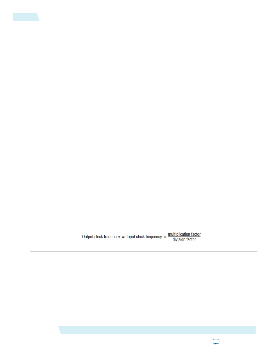
The following figure shows the formula for an output clock frequency.
Figure 5: PLL Output Clock Frequency
The ALTPLL parameter editor calculates the simplest fraction, and displays it in the actual settings column.
For example, if the input clock frequency is 100 MHz, and the requested multiplication and division factors
are 205 and 1025 respectively, the output clock frequency is calculated as 100 × 205/1025=20 MHz. The
actual settings reflect the simplest fraction — the actual multiplication factor is 1, and the actual division
factor is 5. You can use the copy button to copy values from the actual settings to the requested settings.
The actual values of multiplication and division factors are affected when you select Use these clock settings
for the DPA clock or Set up PLL in LVDS mode.
ALTPLL (Phase-Locked Loop) IP Core User Guide
Altera Corporation
ug-altpll
Parameter Settings
10
2014.08.18