Simulating external feedback board delay – Altera ALTPLL (Phase-Locked Loop) IP Core User Manual
Page 8
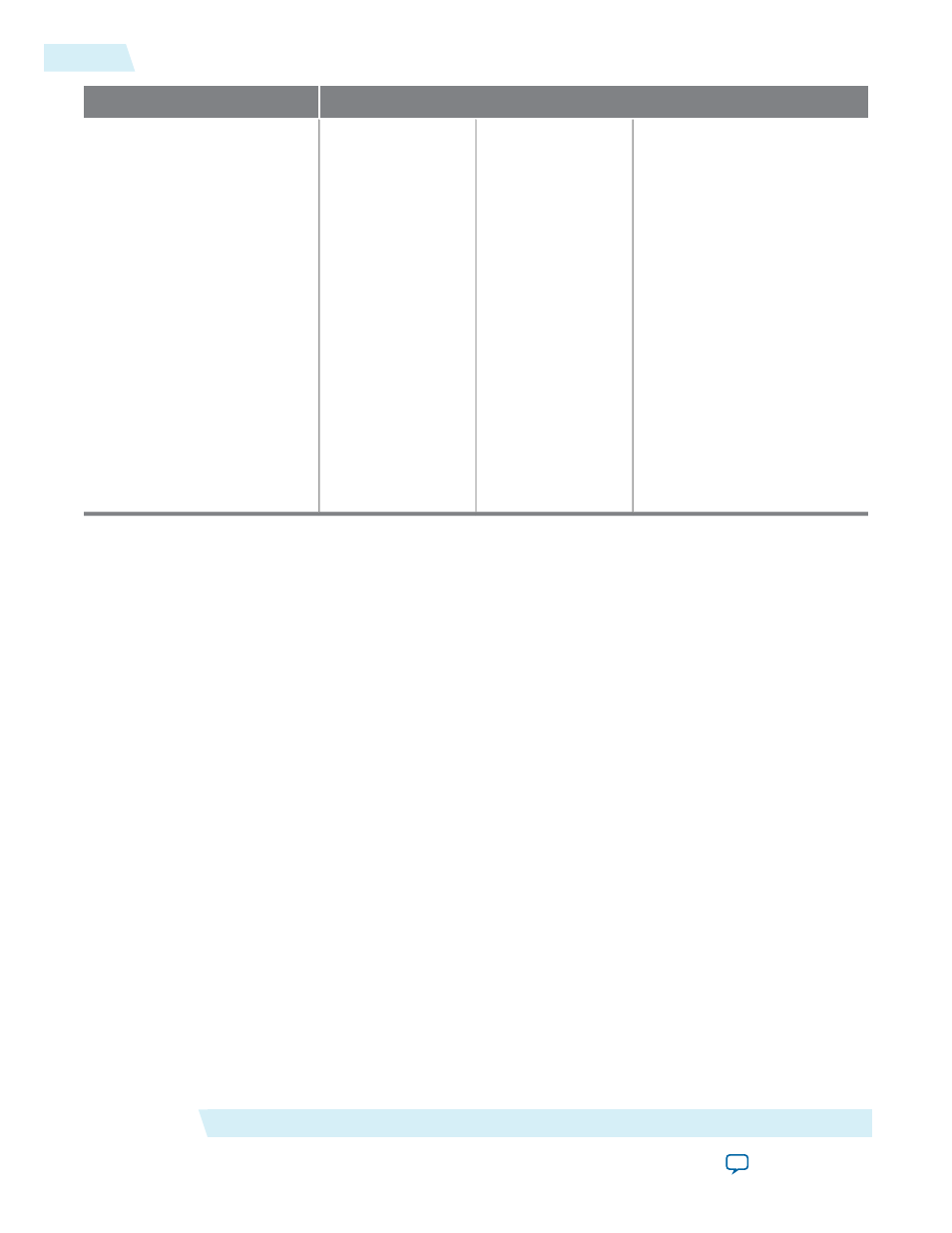
Value
Option
c2
This clock signal is the slow
clock signal that feeds the
synchronization register of the
ALTLVDS IP core.
Output frequency = data rate/
deserialization factor
Phase shift = (-180/deserializa-
tion factor) degrees
Duty cycle = 50%
c1
This clock signal is
the load enable signal
connected to the
rx_
enable
or
tx_enable
port of the ALTLVDS
IP core.
Output frequency =
data rate/deserializa-
tion factor
Phase shift =
[(deserialization
factor – 2)/deserializa-
tion factor] × 360
degrees
Duty cycle = (100/
deserialization factor)
%
c0
This clock signal is
the high-speed serial
clock (fast clock)
signal connected to
the
rx_inclock
or
tx_inclock
port of
the ALTLVDS IP
core.
Output frequency =
data rate
Phase shift = -180
degrees
Duty cycle = 50%
On the Output clocks page
Related Information
Simulating External Feedback Board Delay
The PLL external feedback board delay option is available for Arria GX, Cyclone, HardCopy series, Stratix,
Stratix GX, Stratix II, and Stratix II GX device families only.
The functional and timing models of these devices do not support the simulation of external feedback. To
simulate the external feedback mode, perform the following steps:
1. In the Quartus II software, open an existing project or create a new project.
2. On the Assignments menu, click Assignment Editor.
3. In the Category bar, under Timing, click All.
4. In the spreadsheet, double-click an empty row in the To cell and either type in the pin name or click the
arrow to use the Node Finder to search for the external feedback input pin.
5. Double-click the Assignment Name cell, and select PLL External Feedback Board Delay.
6. In the Value cell, double-click and type the amount of time for the signal to propagate between the
external clock output pin through the trace on the board and into the external feedback input pin.
7. Simulate your design.
The behavioral models for the ALTPLL IP core reside in the \quartus\eda\sim_lib directory. The
altera_mf.vhd file contains the VHDL behavioral models and the altera_mf.v file contains the Verilog HDL
behavioral models. The behavioral model does not perform parameter error checking, so you must specify
valid values.
ALTPLL (Phase-Locked Loop) IP Core User Guide
Altera Corporation
ug-altpll
Simulating External Feedback Board Delay
8
2014.08.18