Output clocks, Parameter settings – Altera ALTPLL (Phase-Locked Loop) IP Core User Manual
Page 9
Output Clocks
The PLL can generate a number of clock output signals depending on the PLL type and the device family
that you select in the ALTPLL parameter editor. For example, in a Stratix IV device, a Left_Right PLL can
generate seven clock output signals, and a Top_Bottom PLL can generate as many as 10 clock output signals.
The generated clock output signals are used to clock the core or external blocks outside of the core.
The ALTPLL IP core does not have a dedicated output enable port, you can disable the PLL output. You can
use the
pllena
signal or the
areset
signal to disable the PLL output counters, and thereby disable the PLL
output clocks. Another possible method is to feed the PLL output clock signals to the ALTIOBUF IP core
and use the enable output ports of the resulting buffers to disable the signals.
Parameter Settings
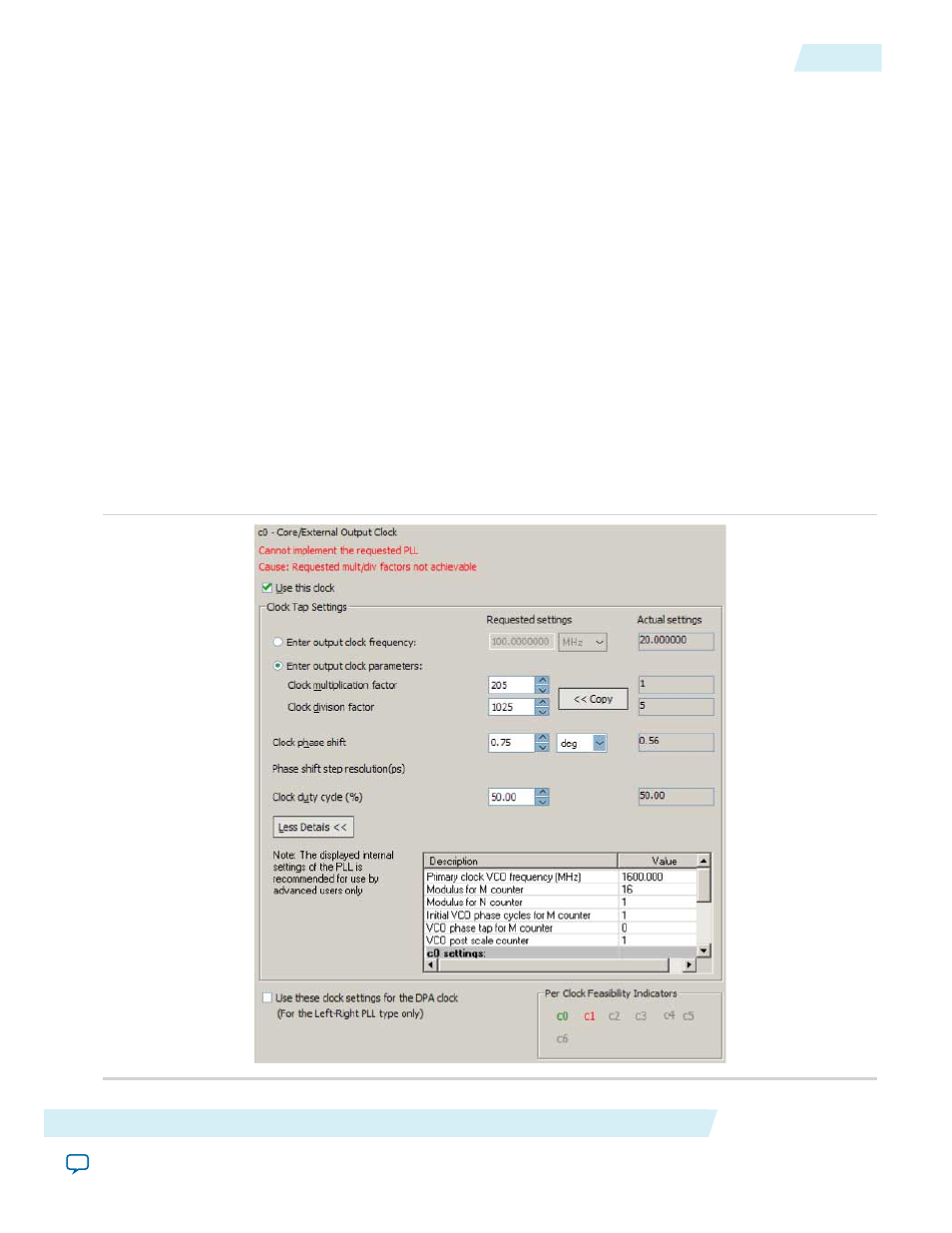
The Output Clocks page of the ALTPLL parameter editor contains the parameter settings for the clock
output signals. The output clock port can be used as a core output clock or an external output clock port.
The core output clock is used to feed the FPGA core and the external output clock is used to feed the dedicated
pins on the FPGA.
The following figure shows a screenshot of the page to configure the
c0
clock output signal of the ALTPLL
IP core.
Figure 4: Output Clocks
Altera Corporation
ALTPLL (Phase-Locked Loop) IP Core User Guide
9
Output Clocks
ug-altpll
2014.08.18