Design example 2: generating clock signals – Altera ALTPLL (Phase-Locked Loop) IP Core User Manual
Page 64
The
ddr_clk
design is now implemented.
Functional Results — Simulate the ddr_clk Design in the ModelSim
®
-Altera Software
This ModelSim design example is for the ModelSim-Altera (Verilog) version. To simulate the design in the
ModelSim-Altera software, follow these steps:
1. Unzip
file to any working directory on your PC.
2. Locate the folder in which you unzipped the files to and open the DDR_CLK.do file in a text editor.
3. In line 1, replace <insert_directory_path_here> with the directory path of the appropriate library files.
For example,
C:/Modeltech_ae/altera/verilog/stratix
4. On the File menu, click Save.
5. Start the ModelSim-Altera software.
6. On the File menu, click Change Directory.
7. Select the folder in which you unzipped the files. Click OK.
8. On the Tools menu, click TCL, and click Execute Macro.
9. Select the DDR_CLK.do file and click Open. The DDR_CLK.do file is a script file for the ModelSim-
Altera software to automate all the necessary settings for the simulation.
10. Verify the results shown in the Waveform Viewer window.
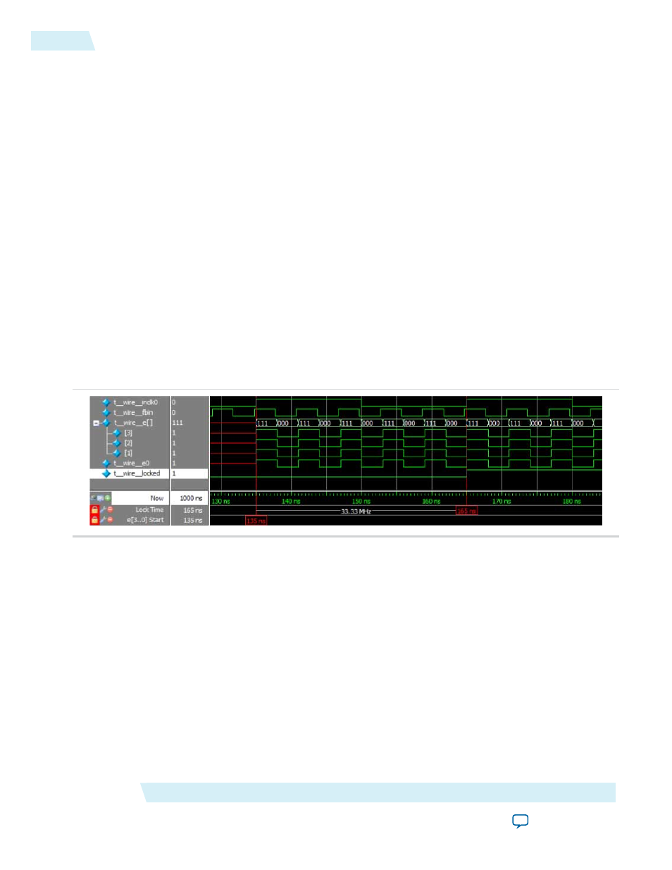
The following figure shows the expected simulation results in the ModelSim-Altera software.
Figure 29: ModelSim Simulation Results
Design Example 2: Generating Clock Signals
This design example uses the ALTPLL IP core to generate and modify internal clock signals. This example
generates three internal clock signals from an external 100-MHz clock signal.
In this example, you perform the following activities:
• Generate 133 MHz, 200 MHz, and 200 MHz clocks that are time shifted by 1.00 ns from a 100 MHz
external input clock using the ALTPLL IP core.
• Implement the
shift_clk
design by assigning the EP1S10F780 device to the project and compiling the
project.
• Simulate the
shift_clk
design.
ALTPLL (Phase-Locked Loop) IP Core User Guide
Altera Corporation
ug-altpll
Functional Results — Simulate the ddr_clk Design in the ModelSim
®
-Altera Software
64
2014.08.18