Clock recovery core, Clock recovery core -4 – Altera DisplayPort MegaCore Function User Manual
Page 65

Arria V/Cyclone V/Stratix V/
Function
USER_LED[7:6]
These LEDs indicate the RX link rate.
• 00 = RBR
• 01 = HBR
• 10 = HBR2
Tip: When creating your own design, note the following design tips:
• The Bitec daughter card has inverted transceiver polarity. When creating your own sink (RX) design,
use the Invert transceiver polarity option to enable or disable inverted polarity.
• The DisplayPort standard reverses the RX and TX transceiver channels to minimize noise for one- or
two-lane applications. If you create your own design targeting the Bitec daughter card, ensure that the
following signals share the same transceiver channel:
•
TX0
and
RX3
•
TX1
and
RX2
•
TX2
and
RX1
•
TX3
and
RX0
Refer to the
assignments.tcl
file for an example of how the channels are assigned in the hardware
demonstration.
Clock Recovery Core
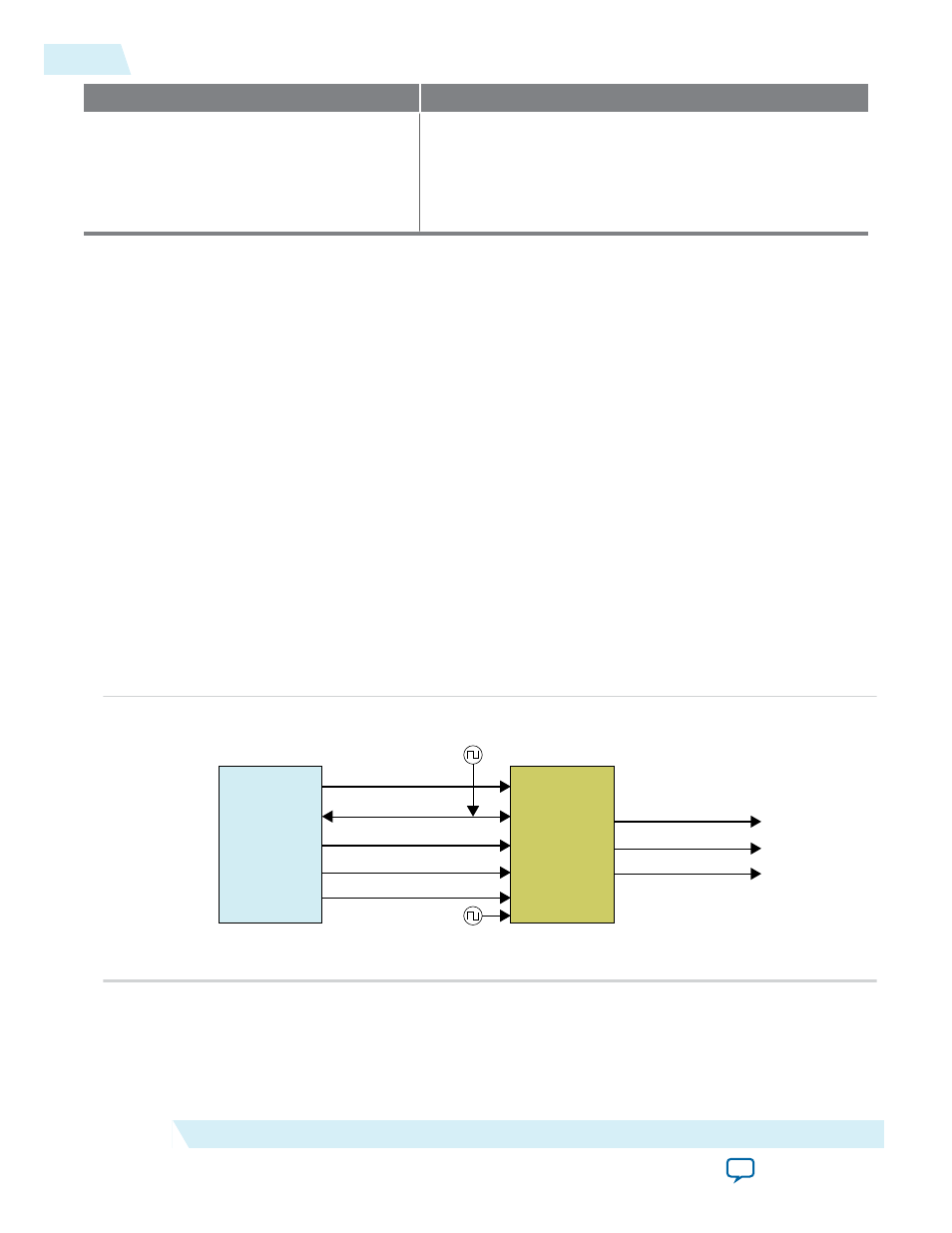
The clock recovery core is a single encrypted module called bitec_clkrec.
Figure 6-3: Clock Recovery Core Integration Diagram
The figure below shows the integration diagram of the clock recovery core.
DisplayPort
IP Core
Clock Recovery
IP Core
RX Video
Clock
Video Output Image Port
RX MSA
RX Link Rate
RX Link Clock
Video Output
Recovered Video Clock
Recovered Video Clock x2
Control
Clock
To synthesize the video pixel clock from the link clock, the clock recovery core gathers information about
the current MSA and the currently used link rate from the DisplayPort sink.
6-4
Clock Recovery Core
UG-01131
2015.05.04
Altera Corporation
DisplayPort IP Core Hardware Demonstration