Zilog Z16C35 User Manual
Page 157
Advertising
Application Note
Interfacing Z80
®
CPUs to the Z8500 Peripheral Family
6-3
6
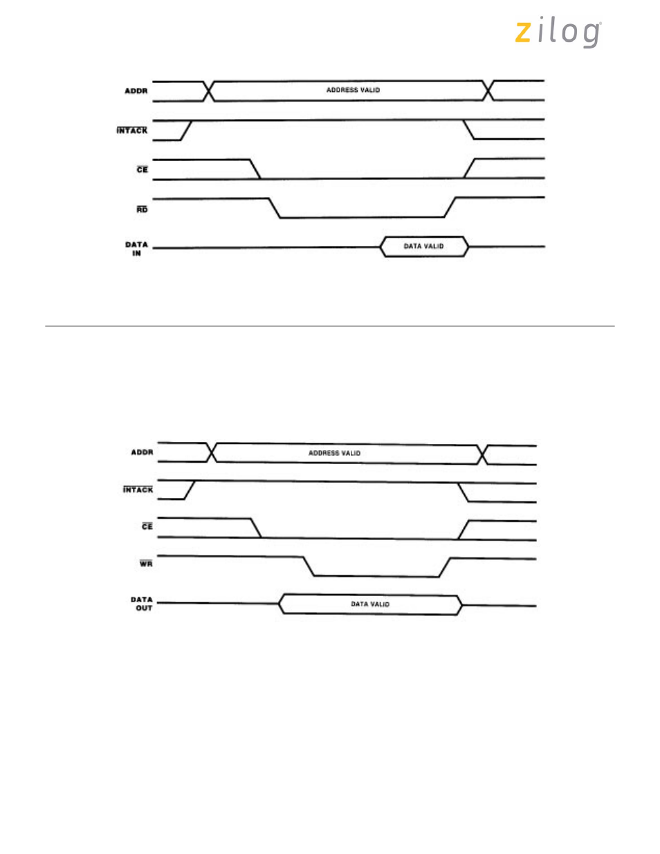
Write Cycle Timing
Figure 2 illustrates the Z8500 Write cycle timing. All
register addresses and /INTACK must remain stable
throughout the cycle. If /CE goes active after /WR goes
active, or if /CE goes inactive before /WR goes inactive,
then the effective Write cycle is shortened. Data must be
available to the peripheral prior to the falling edge of /WR.
Figure 1. Z8500 Peripheral I/O Read Cycle Timing
Figure 2. Z8500 Peripheral I/O Write Cycle Timing
Page 151 of 316
UM011002-0808
Advertising
See also other documents in the category Zilog Sensors:
- S3F94C8 (11 pages)
- S3F80QB (29 pages)
- S3F8S19 (38 pages)
- Z51F6412 (96 pages)
- Z51F6412 (54 pages)
- Z51F6412 (55 pages)
- Z16F6411 (216 pages)
- EZ80F93 (11 pages)
- Z16F6411 (20 pages)
- ZMOT0BSB (582 pages)
- EZ80F93 (13 pages)
- ZMOT0BSB (314 pages)
- Z8F083A (14 pages)
- Z8F2480 (17 pages)
- Z8F082A (18 pages)
- Z8F082A (15 pages)
- Z8F0822 (17 pages)
- Z8F6423 (83 pages)
- Z8F2480 (19 pages)
- Z8F2480 (18 pages)
- Z8F6423 (18 pages)
- Z8F6423 (27 pages)
- Z8F6482 (50 pages)
- EZ80L92 (40 pages)
- EZ80L92 (26 pages)
- EZ80L92 (79 pages)
- EZ80F91GA (469 pages)
- EZ80F915 (411 pages)
- EZ80F91NAA (34 pages)
- EZ80F91 (41 pages)
- EZ80L92 (10 pages)
- eZ80F92 (87 pages)
- Z8FMC16 (26 pages)
- Z16FMC6 (41 pages)
- ZUSBOPTS (38 pages)
- ZUSBOPTS (59 pages)
- Z16FMC6 (520 pages)
- Z16FMC6 (8 pages)
- Z16FMC6 (26 pages)
- ZMOT1AHH (25 pages)
- ZMOT0BSB (34 pages)
- EZ80F915 (78 pages)
- EZ80190 (87 pages)
- EZ80L92 (86 pages)
- EZ80F91GA (127 pages)