Zilog Z16C35 User Manual
Page 306
Application Note
On-Chip Oscillator Design
15-6
PRACTICE: CIRCUIT ELEMENT AND LAY OUT CONSIDERATIONS
The discussion now applies prior theory to the practical
application.
Amplifier and Feedback Resistor
The elements of the circuit, internal to the IC, include the
amplifier, feedback resistor, and output resistance. The
amplifier is modeled as a transconductance amplifier with
a gain specified as I
OUT
/V
IN
(amps per volt).
Transconductance/Gain.
The loop gain AB = gm x Z1,
where gm is amplifier transconductance (gain) in
amps/volt and Z1 is the load seen by the output. AB must
be greater than unity at and about the frequency of
operation to sustain oscillation.
Gain Measurement Circuit.
The gain of the amplifier can
be measured using the circuits of Figures 6 & 7. This may
be necessary to verify adequate gain at the frequency of
interest and in determining design margin.
Gain Requirement vs. Temperature, Frequency and
Supply Voltage.
The gain to start and sustain oscillation
(Figure 8) must comply with:
gm > 4
π
2
f
2
Rq C
IN
C
OUT
t x M
where:
M is a quartz form factor = (1 + C
OUT
/C
IN
+ C
OUT
/C
OUT
)
2
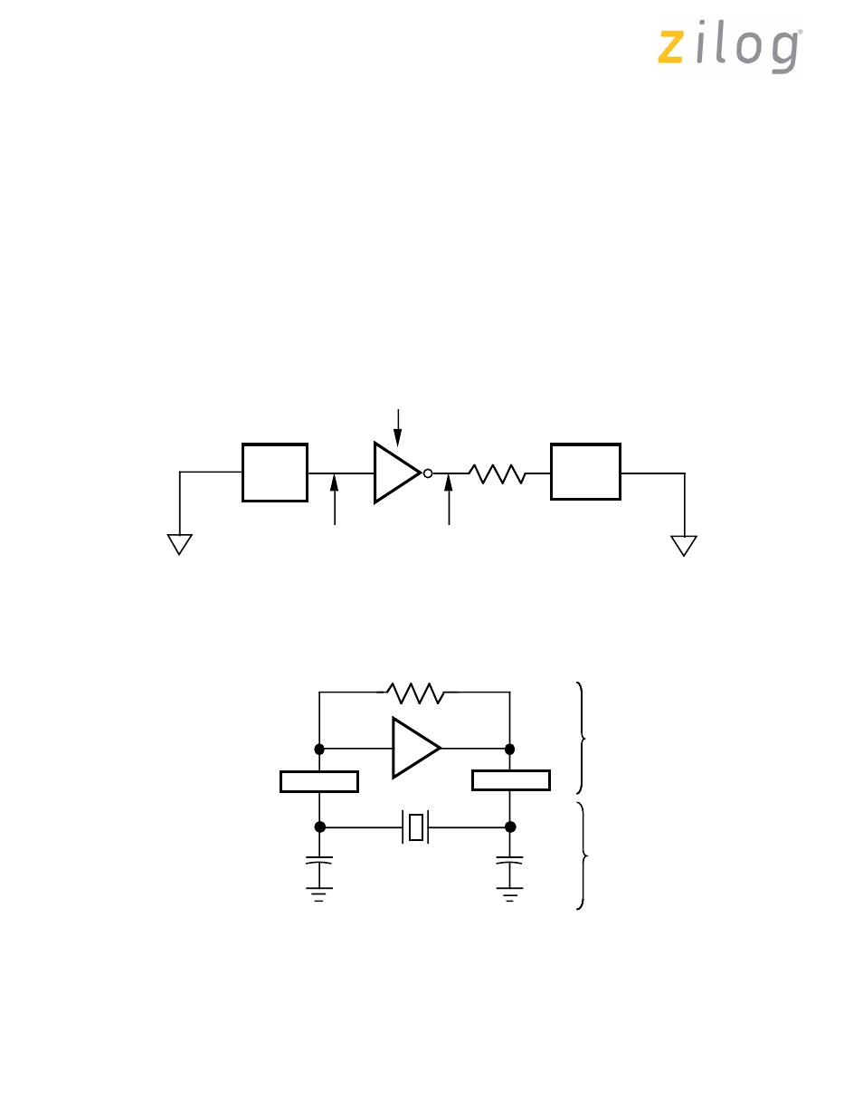
Output Impedance.
The output impedance limits power to
the XTAL and provides small phase shift with load cap C2.
Figure 7. Transconductance (gm) Measurement
IC Under Test
DC Bias
DC Bias
V
V
V
33
Ω
I = (V – V ) /33)
in
out
out
b
out
b
Figure 8. Quartz Oscillator Configuration
VIN
Rq, f
CIN
COUT
Quartz
VOUT
Amplifier
OSC IN
OSC OUT
**
*
Inside chip, feedback resistor biases the amplifier in the high gm region.
**
*
External components typically: CIN = COUT = 30 to 50 pf (add 10 pf pin cap).
Page 300 of 316
UM011002-0808