Continued), Interrupt acknowledge cycle timing – Zilog Z16C35 User Manual
Page 193
Application Note
The Z180™ Interfaced with the SCC at MHZ
7-16
(Continued)
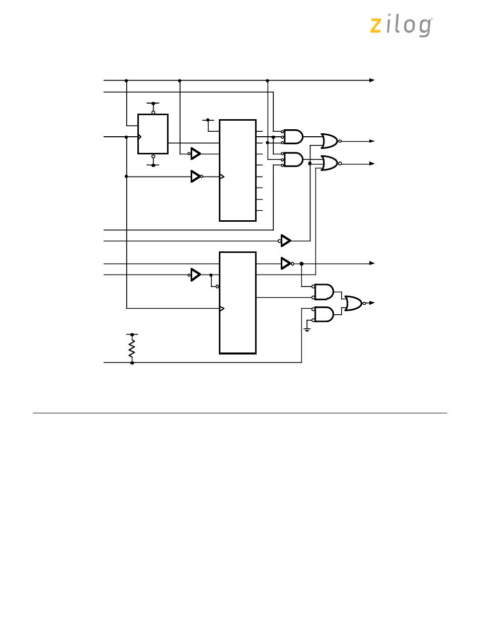
If you are running your system slower than 8 MHz, remove
the HCT74, D-Flip/Flop in front of HCT164. Connect the
inverted CSSCC to the HCT164 B input. This is a required
Flip/Flop because the Z180 timing specification on tIOD1
(Clock High to /IORQ Low, IOC=0) is maximum at 55 ns
This is longer than half the PHI clock cycle. Sample it using
the rising edge of clock, otherwise, HCT164 does not
generate the same signals.
The RESET signal feeds the SCC /RD and /WR through
HCT27 and HCT02 to supply the hardware reset signal. To
reduce the gate count, drop these gates and make the
SCC reset by its software command. The SCC software
reset - 0C0h to Write Register 9, “Hardware Reset
command” has the same effect as hardware reset by
“Hardware.”
Interrupt Acknowledge Cycle Timing
The primary timing differences between the Z180 and
SCC occur in the Interrupt Acknowledge cycle. The SCC
timing parameters that are significant during Interrupt
Acknowledge cycles are in Table 10. The Z180 timing
parameters are in Table 10. The reference numbers in
Tables 10 and 11 refer to Figure 13.
Figure 13. SCC I/O Read/Write Cycle Timing
This circuit works when [(Lower HCT164’s CLK
≠
to Z180 /WAIT
≠
) + tws <tCHW]
D
CK
Q
A
B
/CLR
CK
Q0
Q1
Q2
Q3
Q4
Q5
Q6
Q7
A
B
CLR
CK
Q0
Q1
Q2
Q3
Q4
Q5
Q6
Q7
HCT74
HCT164
HCT04
HCT04
HCT27
HCT02
HCT27
HCT27
HCT04
HCT04
HCT164
HCT04
HCT02
/INTACK
HCT02
HCT02
/CSSCC
/WR
Ø
/RD
/RESET
/MREQ
/M1
Internal
/WAIT
Input
To
Z180
/WAIT
To 85C30
/INTACK
To
85C30
/RD
To
85C30
/WR
To
85C30
/CE
4.7K
Page 187 of 316
UM011002-0808