Zilog Z16C35 User Manual
Page 180
Application Note
The Z180™ Interfaced with the SCC at MHZ
7-3
7
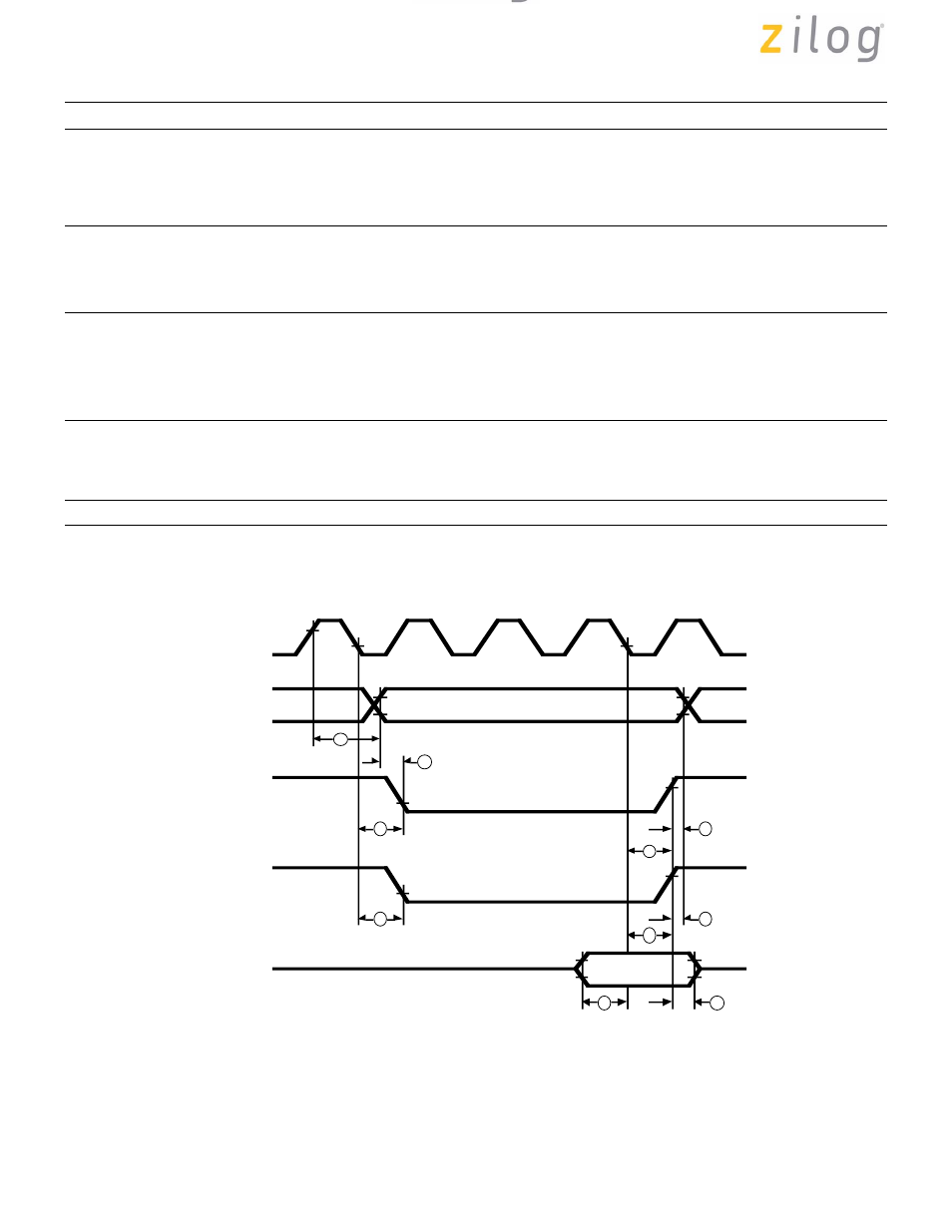
Table 1. Z8018010 Timing Parameters for Opcode Fetch Cycle (Worst Case: Z180 10 MHz)
No
Symbol
Parameter
Min
Max
Units
1
tcyc
Clock Cycle Period
100
ns
2
tCHW
Clock Cycle High Width
40
ns
3
tCLW
Clock Cycle Low Width
40
ns
4
tcf
Clock Fall Time
10
ns
6
tAD
Clock High to Address Valid
70
ns
8
tMED1
Clock Low to /MREQ Low
50
ns
9
tRDD1
Clock Low to /RD Low
50
ns
11
tAH
Address Hold Time
10
ns
12
tMED2
Clock Low to /MREQ High
50
ns
15
tDRS
Data to Clock Setup
25
ns
16
tDRH
Data Read Hold Time
0
ns
22
tWRD1
Clock High to /WR Low
50
ns
23
tWDD
Clock Low to Write Data Delay
60
ns
24
tWDS
Write Data Setup to /WR Low
15
ns
25
tWRD2
Clock Low to /WR High
50
ns
26
tWRP
/WR Pulse Width
110
ns
27
tWDH
/WR High to Data Hold Time
10
ns
Note:
Parameter numbers in this table are in the Z180 technical manual.
Figure 2. Z180 Memory Read Cycle Timing (One Wait State)
7
6
8
9
12
11
13
11
15
16
Ø
Address
/MREQ
/RD
Data
Read Data
T1
T2
Tw
T3
T1
Page 174 of 316
UM011002-0808