Zilog Z16C35 User Manual
Page 259
Application Note
Using SCC with Z8000 in SDLC Protocol
12-4
SYSTEM INTERFACE
(Continued)
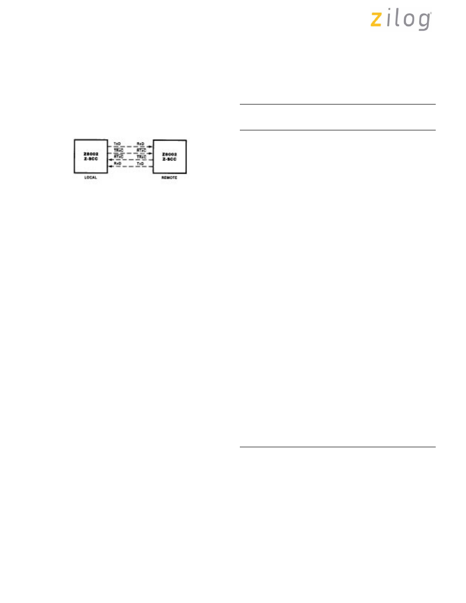
Two Z8000 Development Modules containing SCCs are
connected as shown in Figure 4 and Figure 5. The
Transmit Data pin of one is connected to the Receive Data
pin of the other and vice versa. The Z8002 is used as a
host CPU for loading the modules; memories with software
routines.
The Z8002 CPU can address either of the two bytes
contained in 16-bit words. The CPU uses an even address
(16 bits) to access the most significant byte of a word and
an odd address for the least significant byte of a word.
When the Z8002 CPU uses the lower half of the
Address/Data bus (AD7-AD0 the least significant byte) for
byte read and write transactions during I/O operations,
these transactions are performed between the CPU and
I/O ports located at odd I/O addresses. Since the SCC is
attached to the CPU on the lower half of the A/D bus, its
registers must appear to the CPU at odd I/O addresses. To
achieve this, the SCC can be programmed to select its
internal registers using lines AD5-AD1. This is done either
automatically with the Force Hardware Reset command in
WR9 or by sending a Select Shift Left Mode command to
WR0B in channel B of the SCC. For this application, the
SCC registers are located at I/O port address “Fexx”. The
Chip Select signal (/CSO) is derived by decoding I/O
address “FE” hex from lines AD15-AD8 of the controller.
To select the read/write registers automatically, the SCC
decodes lines AD5-AD1 in Shift Left mode. The register
map for the SCC is depicted in Table 1.
Figure 4. Block Diagram of Two Z8000 CPUs
Table 1. Register Map
Address
Write
Read
(Hex)
Register
Register
FE01
WR0B
RR0B
FE03
WR1B
RR1B
FE05
WR2
RR2B
FE07
WR3B
RR3B
FE09
WR4B
FE0B
WR5B
FE0D
WR6B
FE0F
WR7B
FE11
B DATA
B DATA
FE13
WR9
FE15
WR10B
RR10B
FE17
WR11B
FE19
WR12B
RR12B
FE1B
WR13B
RR13B
FE1D
WR14B
FE1F
WR15B
RR15B
FE21
WR0A
RR0A
FE23
WR1A
RR1A
FE25
WR2
RR2A
FE27
WR3A
RR3A
FE29
WR4A
FE2B
WR5A
FE2D
WR6A
FE2F
WR7A
FE31
A DATA
A DATA
FE33
WR9
FE35
WR10A
RR10A
FE37
WR11A
FE39
WR12A
RR12A
FE3B
WR13A
RR13A
FE3D
WR14A
FE3F
WR15A
RR15A
Page 253 of 316
UM011002-0808