4 i/o connector pin arrangement and i/o circuits, I/o connector pin arrangement – Yaskawa MP940 User Manual
Page 195
5.3 Connection Methods
5-23
5
5.3.4 I/O Connector Pin Arrangement and I/O Circuits
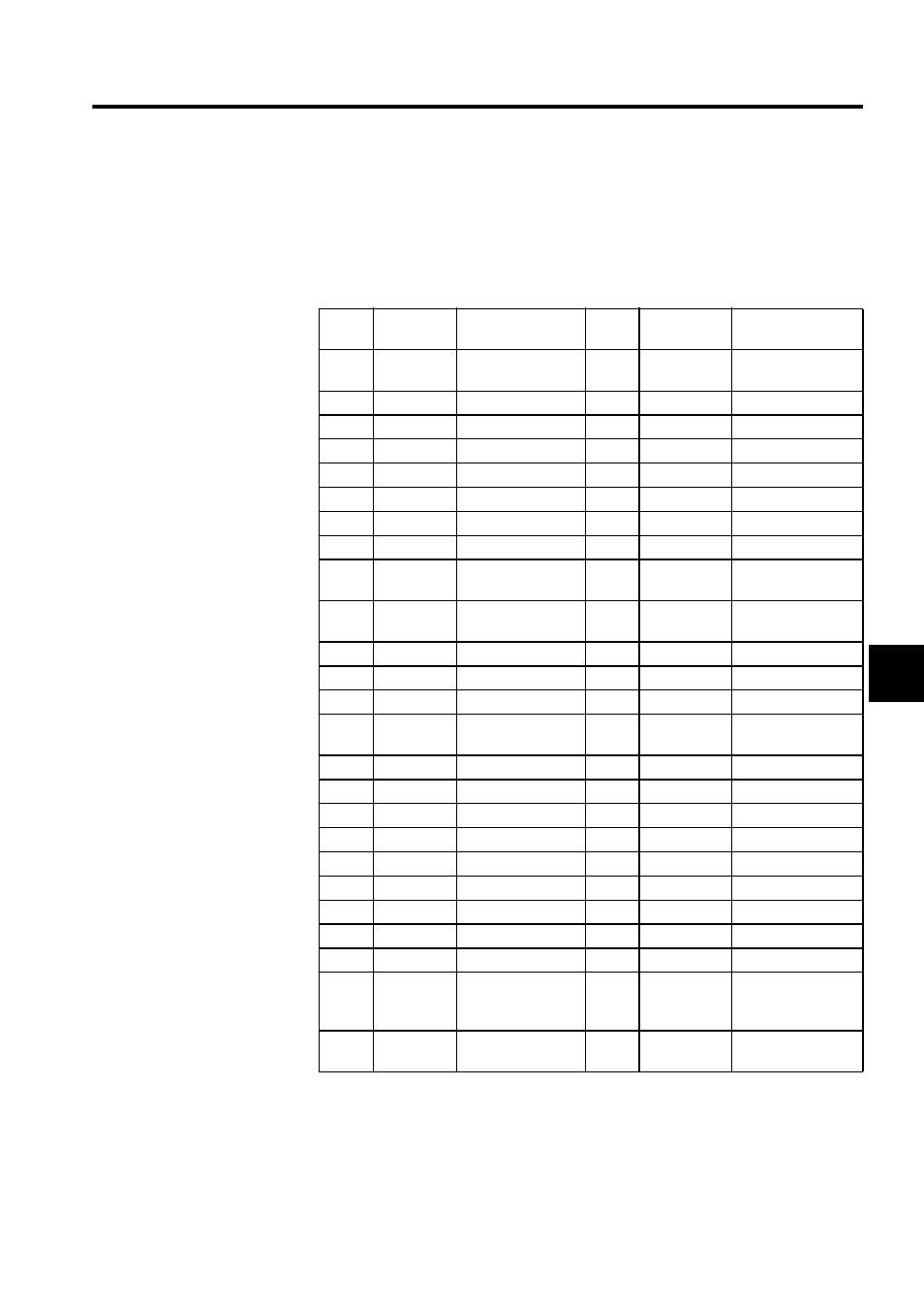
I/O Connector Pin Arrangement
The names of the I/O connector terminals and their functions are shown in the following
table.
No.
Signal
Name
Remarks
No.
Signal Name
Remarks
1
AO
Analog output
26
AO_GND
Analog output
ground
2
27
3
28
4
PA+
A pulse positive
29
PB+
B pulse positive
5
PA-
A pulse negative
30
PB-
B pulse negative
6
GND
Pulse input ground
31
GND
Pulse input ground
7
32
8
33
9
PILC 5 V
PI latch input com-
mon (5 V)
34
PILC 12 V
PI latch input com-
mon (12 V)
10
PILC 24V
PI latch input com-
mon (24 V)
35
PIL
PI latch input com-
mon
11
36
12
37
13
24 VDC
DI power supply
38
24 VDC
DI power supply
14
DI_00
DI_00 input (DI
interrupt)
39
DI_01
DI_01 input
15
DI_02
DI_02 input
40
DI_03
DI_03 input
16
DI_04
DI_04 input
41
DI_05
DI_05 input
17
DI_06
DI_06 input
42
DI_07
DI_07 input
18
43
19
44
20
24 VDC
DO power supply
45
24 VDC
DO power supply
21
DO_00
DO_00 output
46
DO_01
DO_01 output
22
DO_02
DO_02 output
47
DO_03
DO_03 output
23
DO_04
DO_04 output
48
DO_05
DO_05 output
24
DO_06
DO_06 output
49
DO_07
DO_07output
(counter coinci-
dence output)
25
DO_GND
DO ground (0 V)
50
DO_GND
DO
ground (0 V)