Altera JESD204B IP User Manual
Page 106
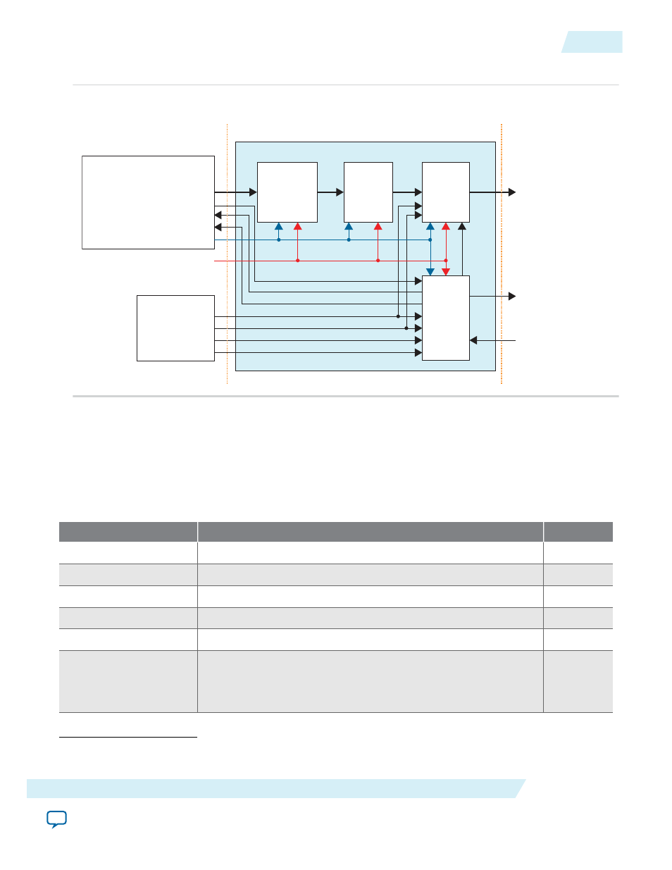
Figure 5-9: RX Path Assembler Block Diagram
Deassembling
Multiplexing
RX Control
jesd204_rx_link_datain[(L*32)-1:0]
jesd204_rx_link_data_valid
jesd204_rx_linkdata_ready
jesd204_rx_linkerror
Configuration Register Settings
rxframe_clk
rxframe_rst_n
rxlink_clk
rxlink_rst_n
Control Unit
JESD204B IP Core Data Link Layer
Data
Bus
Data
Bus
Data
Bus
Data
Bus
jesd204_rx_dataout
[OUTPUT_BUS_WIDTH-1:0]
JESD204B Transport Layer RX Block
jesd204_rx_data_valid
jesd204_rx_data_ready
Interface with
Avalon-ST
Interfaces with JESD204B IP Core
Data Link Layer and Control Unit
Parameter L, M, F, N, N’,S,
F1_FRAMECLK_DIV,
F2_FRAMECLK_DIV
Tail Bits
Dropping
• Tail bit dropping block—drops padded tail bits in the incoming data (
jesd204_rx_link_datain
).
• Deassembling block—rearranges the resulting data bits in a specific way according to the mapping
scheme (refer to
).
• Multiplexing block—sends the multiplexed data to the Avalon-ST interface, determined by certain
control signals from the RX control block.
Table 5-11: Deassembler Parameter Settings
Parameter
Description
Value
L
Number of lanes per converter device.
1–8
F
Number of octets per frame.
1, 2, 4, 8
CS
Number of control bits or conversion sample.
0–3
N
Number of conversion bits per converter.
12-16
N'
Number of transmitted bits per sample in the user data format.
16
F1_FRAMECLK_DIV Only applies to cases where F=1.
The divider ratio on the
frame_clk
. The deassembler always uses the
post-divided frame_clk (rxframe_clk).
(34)
1, 4
(34)
Refer to the
to set the desired frame clock frequency with different FRAMECLK_DIV and F
parameter values.
UG-01142
2015.05.04
RX Path
5-25
JESD204B IP Core Design Guidelines
Altera Corporation