Mif rom – Altera JESD204B IP User Manual
Page 132
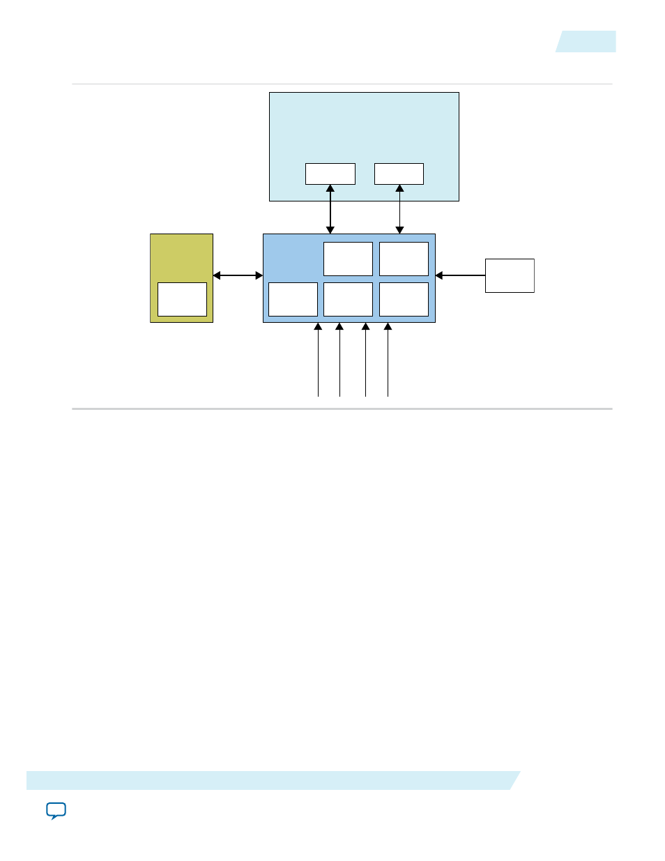
Figure 5-20: Dynamic Reconfiguration Block Diagram (For 20 nm Device Families—Arria 10)
JESD204B IP Core (Duplex)
CSR
PHY
SPI Master
Clock MIF
ROM
DAC MIF
ROM
ADC MIF
ROM
JESD MIF
ROM
Control Unit
PLL MIF
ROM
PLL
Reconfiguration Avalon-MM
Avalon-MM
Avalon-MM
rec
onfig
run
time_lmf
run
time_datar
at
e
cu_busy
Avalon-MM
PHY MIF
ROM
The MIF ROM content for maximum and downscale configuration:
• PLL MIF ROM—contains the PLL counter, charge pump, and bandwidth setting.
• JESD MIF ROM—contains the LMF information.
• PHY MIF ROM—contains the transceiver channel and PLL setting.
• ADC MIF ROM—contains the ADC converter setting.
• DAC MIF ROM—contains the DAC converter setting.
• CLK MIF ROM—contains the device clock setting.
MIF ROM
You need to generate two MIF files for each reconfigurable IP core as shown in
, and merge them into a single MIF file for each IP core. The following section shows the MIF file
format.
Core PLL
The MIF format is fixed by the PLL. You need to generate two PLLs with maximum and downscale
setting to get these two MIF files. Then, merge the files into one (core_pll.mif). Only the PLL with
maximum configuration is used in final compilation.
Maximum Configuration MIF
WIDTH=32;
DEPTH=92;
ADDRESS_RADIX=UNS;
UG-01142
2015.05.04
MIF ROM
5-51
JESD204B IP Core Design Guidelines
Altera Corporation