Altera JESD204B IP User Manual
Page 95
Signal
Clock Domain
Direction
Description
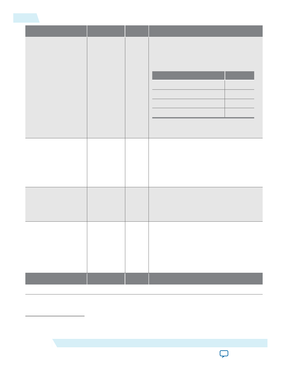
jesd204_tx_link_
datain[(L*32)-1:0]
txlink_clk
Output
Indicates transmitted data from the transport
layer to the DLL at
txlink_clk
clock rate, where
four octets are packed into a 32-bit data width per
lane. The data format is big endian. The table
below illustrates the data mapping for L = 4:
jesd204_tx_link_datain [x:y]
Lane
[31:0]
0
[63:32]
1
[95:64]
2
[127:96]
3
Connect this signal to the TX DLL
jesd204_tx_
link_data[]
input pin.
jesd204_tx_link_
data_valid
txlink_clk
Output
Indicates whether the
jesd204_tx_link_
datain[]
is valid or invalid.
• 0—
jesd204_tx_link_datain[]
is invalid
• 1—
jesd204_tx_link_datain[]
is valid
Connect this signal to the TX DLL
jesd204_tx_
link_valid
input pin.
jesd204_tx_link_
early_ready
(30)
txlink_clk
Input
Indicates that the DLL requires valid data at the
subsequent implementation-specific duration.
Connect this signal to the TX DLL
jesd204_tx_
frame_ready
output pin.
jesd204_tx_link_
error
txlink_clk
Output
Indicates an error at the Avalon-ST source
interface. Specifically, this signal is asserted when
jesd204_tx_data_valid
= "0" while
jesd204_
tx_data_ready
= "1". The DLL subsequently
reports this error to the CSR block.
Connect this signal to the TX DLL
jesd204_tx_
frame_error
input pin.
Signal
Clock Domain
Direction
Description
CSR in DLL
(30)
If a JESD device of No Multiple-Converter Device Alignment, Single-Lane (NMCDA-SL) class is deployed,
Altera recommends that you tie this input signal to "1".
5-14
TX Path
UG-01142
2015.05.04
Altera Corporation
JESD204B IP Core Design Guidelines