Memory block (rom) – Altera JESD204B IP User Manual
Page 119
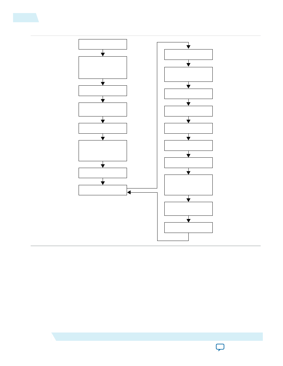
Figure 5-15: Control Unit Process Flow
Power-Up and Reset
Assert Transceiver
(user-triggered),
Frame, and CSR Reset
SPI Configuration
Assert Link, Frame, and
CSR Reset
Deassert Transceiver Reset
Deassert CSR Reset,
followed by Link and
Frame Reset
INIT Done
IDLE
Start Reconfiguration
Assert Link and
Frame Transceiver Reset
SPI Reconfiguration
LMF Reconfiguration
PLL Reconfiguration
Transceiver Reconfiguration
Deassert Transceiver Reset
Deassert Link and Frame
Reset
Clear
tx_err, rx_err0, and rx_err1
status registers
Reconfiguration Done
reconfig = 1’b1
Memory Block (ROM)
The control unit is a finite state machine (FSM) that works with multiple memory blocks (ROMs).
Each ROM holds the configuration data required to configure the external converter or clock devices for
each SPI slave. A memory initialization file (MIF) contains the initial values for each address in the
memory. Each memory block requires a separate file. The MIF can be created in the Quartus II software
text editor tool.
5-38
Memory Block (ROM)
UG-01142
2015.05.04
Altera Corporation
JESD204B IP Core Design Guidelines