Programmable lmfc offset, Programmable lmfc offset -5, Figure 6-4: selecting legal rbd offset value – Altera JESD204B IP User Manual
Page 143: Sync_n signal on page 4-14
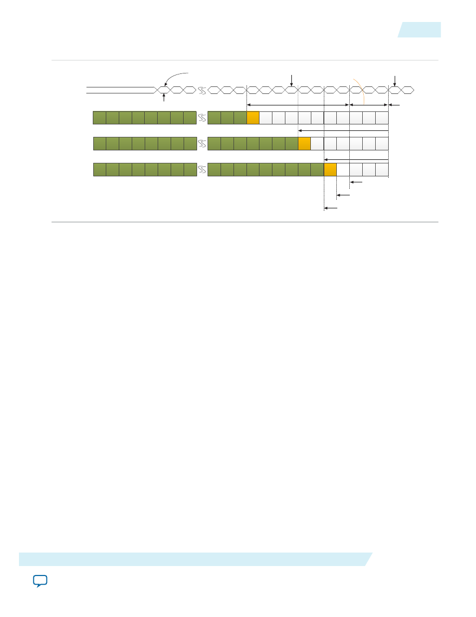
Figure 6-4: Selecting Legal RBD Offset Value
First LMFC
boundary
Free running LMFC counter
0
1
2
3
4
5
6
0
1
2
3
4
5
6
7
K
K
K
K
K
K
K
K
Earliest arrival
lane
D
D
D
D
0
1
RBD count = 7
K
K
K
K
K
K
K
K
Latest arrival
lane
R
D
D
Next LMFC
boundary
K
K
K
K
K
K
K
K
K
Aligned
outputs on all
lanes
K
R
D
D
RBD Elastic
Buffers Released
Set csr_rbd_offset = 5
7 LMFC counts with
reference to the
next LMFC boundary
Internal LMFC counter resets
7
Current LMFC
boundary
D
D
D
D
D
D
D
D
2
D
D
D
D
K
K
K
K
K
K
K
RBD elastic buffer size = 8
R
K
K
K
RBD Elastic
buffers released
at LMFC
boundary when
csr_rbd_offset=0
K
K
K
K
K
K
K
Legal csr_rbd_offset=4
within RBD elastic buffer size
Illegal csr_rbd_offset=1, 2, 3
exceeding RBD elastic buffer size
Internal
LMFC Counter
RBD elastic buffer size exceeded
and causes lane deskew error
Because the IP core does not report the position of the earliest lane arrival with respect to the LMFC
boundary, you should perform multiple power cycles to observe the RBD count and tune the RBD offset
accordingly until no lane de-skew error occurs. From the example in the figure above, the recommended
RBD offset value is 4 or 5. Setting RBD offset to 1, 2 or 3 is illegal because this exceeds the RBD elastic
buffer size for the F and K configurations.
Related Information
on page 4-14
Programmable LMFC Offset
If your JESD204B subsystem design has deterministic latency issue, the programmable LMFC offset in the
TX and RX IP cores provides flexibility to ensure that deterministic latency can be achieved.
The TX LMFC offset can align the TX LMFC counter to the LMFC counter in DAC; the RX LMFC offset
can align the RX LMFC counter to the LMFC counter in ADC. Phase offset between the TX and RX
LMFC counters in the both ends of the JESD204B link contributes to deterministic latency uncertainty.
The phase offset is caused by:
• SYSREF trace length mismatch in the PCB between the TX and RX devices (FPGA and converters).
• delay differences in resetting the LMFC counter when SYSREF pulses are detected by the FPGA and
converter devices.
The RX device in the JESD204B link is responsible for deterministic latency adjustments. The following
figure illustrates the adjustments that you can make to the RX LMFC offset using the csr_lmfc_offset field
in the
syncn_sysref_ctrl
register. This is an alternative to using csr_rbd_offset to achieve deterministic
latency.
UG-01142
2015.05.04
Programmable LMFC Offset
6-5
JESD204B IP Core Deterministic Latency Implementation Guidelines
Altera Corporation