Altera JESD204B IP User Manual
Page 92
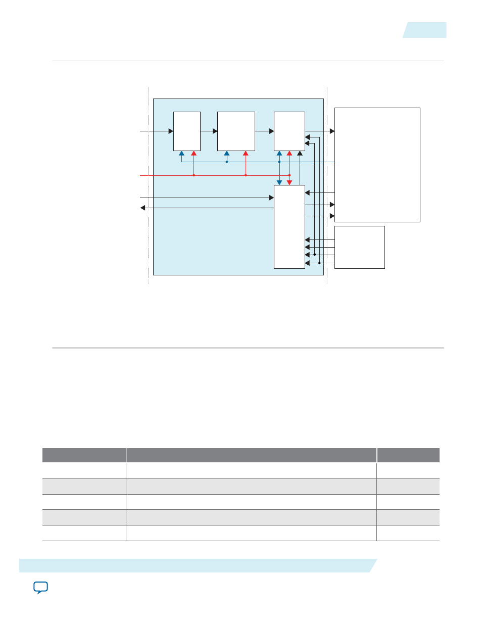
Figure 5-3: TX Path Assembler Block Diagram
Tail Bits
Padding
Assembling
Multiplexing
TX Control
jesd204_tx_link_datain[(L*32)-1:0]
Configuration Register Settings
jesd204_tx_link_early_ready
jesd204_tx_link_data_valid
jesd204_tx_link_error
txframe_clk
txframe_rst_n
txlink_clk
txlink_rst_n
Control Unit
JESD204B IP Core
Data Link Layer
Data
Bus
Data
Bus
Data
Bus
Data
Bus
jesd204_tx_datain
[DATA_BUS_WIDTH-1:0]
(1)
JESD204B Transport Layer TX Block
Interface with
Avalon-ST
jesd204_tx_data_valid
jesd204_tx_data_ready
Interfaces with JESD204 IP Core
Data Link Layer and Control Unit
Parameter L, M, F, N, N’,S,
F1_FRAMECLK_DIV,
F2_FRAMECLK_DIV
Note:
1. The DATA_BUS_WIDTH value is the data input bus width size, which depends on the F and L parameter.
bus_width=M*S*N
F=(M*S*N_PRIME)/(8*L)
M*S=(8*F*L)/N_PRIME
bus_width=(8*F*L*N)/N_PRIME
• Tail bits padding block—pads incoming data (
jesd204_tx_datain
) with "0" if N < 16, so that the
padded data is 16 bits per sample.
• Assembling block—arranges the resulting data bits in a specific way according to the mapping scheme
).
• Multiplexing block—sends the multiplexed data to the DLL interface, determined by certain control
signals from the TX control block.
Table 5-4: Assembler Parameter Settings
Parameter
Description
Value
L
Number of lanes per converter device.
1–8
F
Number of octets per frame.
1, 2, 4, 8
CS
Number of control bits or conversion sample.
0–3
N
Number of conversion bits per converter.
12-16
N'
Number of transmitted bits per sample in the user data format.
16
UG-01142
2015.05.04
TX Path
5-11
JESD204B IP Core Design Guidelines
Altera Corporation