Spi programming, Converter and fpga operating conditions, Signal polarity and fpga pin assignment – Altera JESD204B IP User Manual
Page 149: Spi programming -2, Converter and fpga operating conditions -2, Signal polarity and fpga pin assignment -2
Check these items:
• Turn off the scrambler and descrambler options as needed.
• Use single lane configuration and K = 32 value to isolate multiple lane alignment issue.
• Use Subclass 0 mode to isolate SYSREF related issues like setup or hold time and frequency of SYSREF
pulse.
SPI Programming
The SPI interface configures the converter. Hence, it is important to check the SPI programming sequence
and register bit settings for the converter. If you use the MIF to store the SPI register settings of the
converter, mistakes may occur when modifying the MIF, for example, setting a certain bit to "1" instead of
"0", missing or extra bits in a MIF content row.
Check these items:
• For example, in the ADI AD9250 converter, Altera recommends that you first perform register bit
setting for the scramble (SCR) or lane (L) register at address 0x6E before setting the quick configura‐
tion register at address 0x5E.
• Determine that each row of the MIF has the same number of bits as the data width of the ROM that
stores the MIF.
Converter and FPGA Operating Conditions
The transceiver channels at the converter and FPGA are bounded by minimum and maximum data rate
requirements. Always check the most updated device data sheet for this info. For example, the Arria V GT
device has a minimum data rate of 611 Mbps.
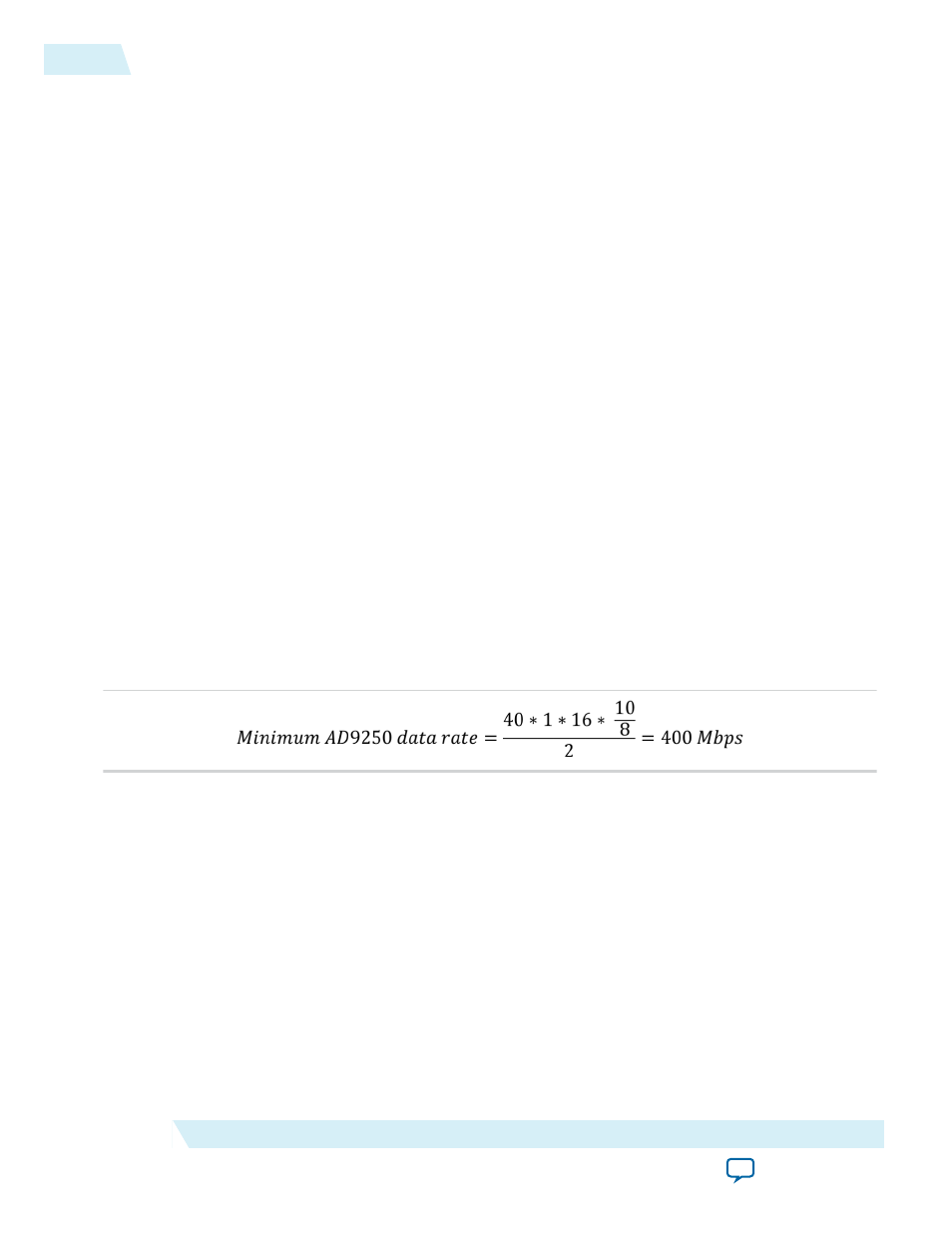
Ensure that the sampling rate of the converter is within the minimum and maximum requirements. For
example, the ADC AD9250 has a minimum sampling rate of 40 Msps. For L = 2, M = 1 configuration, the
minimum data rate of this ADC is calculated this way:
The minimum data rate for the JESD204B link is effectively 611 Mbps.
Check these items:
• Reduce the data rate or sampling clock frequency if your targeted operating requirement does not
work.
• Verify the minimum and maximum data rate requirements in the device manufacturer's data sheet.
Signal Polarity and FPGA Pin Assignment
Verify that the transceiver channel pin assignments—
SYNC_N
and SYSREF (for Subclass 1 only)—device
clock, and SPI interface are correct. Also verify the signal polarity of the differential pairs like
SYNC_N
and
transceiver channels are correct.
7-2
SPI Programming
UG-01142
2015.05.04
Altera Corporation
JESD204B IP Core Debug Guidelines