Dk d d – Altera JESD204B IP User Manual
Page 146
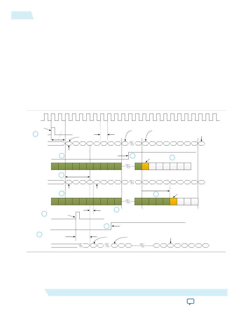
Figure 6-7: Example of Reducing LMFC Phase Offset between TX and RX LMFC Counter
Sequence of events in the diagram:
1. SYSREF pulse arrives at the FPGA IP core port,
tx_sysref
.
2. The IP core's internal LMFC counter resets after two link clock cycles.
3. SYSREF pulse is sampled by the DAC.
4. The DAC's internal LMFC counter resets after a deterministic delay.
5. The LMFC phase offset is ~3.5 link clock cycles.
6. The DAC deasserts SYNC_N at the LMFC boundary.
7. SYNC_N deassertion is detected by the JESD204B IP core.
8. Because SYNC_N deassertion is detected after the second LMFC boundary at the FPGA, ILAS
transmission begins at the third LMFC boundary.
9. The csr_lmfc_offset is set to 4. This delays the TX LMFC boundary by 4 link clock cycles. If
csr_lmfc_offset is set to 5, the TX LMFC boundary is delayed by 3 link clock cycles.
10.The LMFC phase offset between the TX and RX LMFC reduces to 0.5 link clock cycle.
First LMFC
boundary
SYSREF pulse is
sampled by DAC
2 link clock cycle deterministic delay from
SYSREF sampled high to the first LMFC boundary
Free running LMFC counter
Internal
LMFC Counter
0
1
0
1
2
0
1
2
3
4
5
SYNC_N deasserted at
the LMFC boundary
1 link clock period
= LMFC count
7
Third LMFC
boundary
Free running
LMFC counter
0
1
2
3
4
5
6
7
0
1
2
3
4
5
6
7
0
7
SYSREF pulse is
sampled by FPGA
IP core
SYNC_N transmitted
by DAC
0
SYNC_N deassertion is
detected by the IP core
SYNC_N
arrival at TX
K
K
K
K
K
R
K
K
K
K
K
L Transmit
lanes
D
D
D
D
K
D
D
ILAS transmission by the FPGA
Internal LMFC counter resets
csr_lmfc_offset=0
First LMFC
boundary
Second LMFC
boundary
Third LMFC
boundary
6
Fourth LMFC
boundary
Link clock
Internal
LMFC Counter
Deterministic delay from
SYSREF sampled high to
the first LMFC boundary
LMFC phase offset
Free running
LMFC counter
4
5
6
7
0
1
2
3
4
5
6
7
0
1
2
3
4
3
4
Internal
LMFC Counter
Internal LMFC counter resets
csr_lmfc_offset=4
First LMFC boundary
at new location
K
K
K
K
K
R
K
K
K
K
K
L Transmit
lanes
D
K
D
D
K
K
K
Reduced LMFC
phase offset
K
LMFC boundary is
delayed by 4 link clock
tx_sysref
1
2
3
4
5
6
7
8
9
10
9
Second LMFC
boundary
ILAS transmission by the FPGA
Alternative to tuning RBD offset at the DAC, adjusting TX LMFC offset in the FPGA helps you to achieve
deterministic latency. You should perform multiple power cycles and read the RBD counts at the DAC to
determine whether deterministic latency is achieved and RBD elastic buffer size has not exceeded.
6-8
Programmable LMFC Offset
UG-01142
2015.05.04
Altera Corporation
JESD204B IP Core Deterministic Latency Implementation Guidelines