Rx error reporting – Altera JESD204B IP User Manual
Page 116
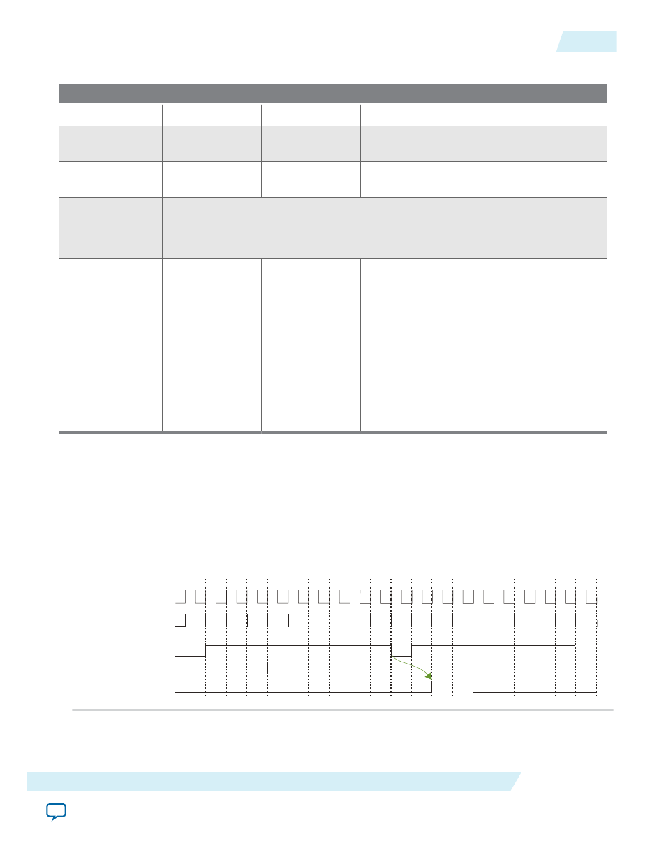
Table 5-16: Data Mapping for F=8, L=4
F = 8
Lane
L3
L2
L1
L0
Data In linkclk
T0
{F24, F25, F26,
F27}
{F16, F17, F18,
F19}
{F8, F9, F10, F11} {F0, F1, F2, F3}
Data In linkclk
T1
{F28, F29, F30,
F31}
{F20, F21, F22,
F23}
{F12, F13, F14,
F15}
{F4, F5, F6, F7}
Supported M
and S
M*S=16 for F=8, L=4
F=8 supports either (case1: M=1, S=16), (case2: M=2, S=8), (case3: M=4, S=4), (case4:
M=8, S=2) or (case5: M=16, S=1)
F=8
jesd204_rx_
dataout[255:0] =
{{F3031,
F28F29,F26F27,
F24F25},{F22F23,
F20F21,F18F19,
F16F17},{F14F15,
F12F13,
F10F11,F8F9},
{F6F7,F4F5,
F2F3,F0F1}}
Case1: M=1, S=16 {M0S15, M0S14, M0S13, M0S12, M0S11,
M0S10, M0S9, M0S8, M0S7, M0S6, M0S5,
M0S4, M0S3, M0S2, M0S1, M0S0}
RX Error Reporting
For RX path error reporting, the transport layer expects the AL to always be ready to sample the RX data
(as indicated by the
jesd204_rx_data_ready
signal equal to "1") as long as the
jesd204_rx_data_valid
remains asserted. If the
jesd204_rx_data_ready
signal unexpectedly deasserts, the transport layer
reports the error to the DLL by asserting the
jesd204_rx_link_error
signal, as shown in the timing
diagram below.
Figure 5-12: RX Error Reporting
rxframe_clk
rxlink_clk
jesd204_rx_link_error
jesd204_rx_data_valid
jesd204_rx_data_ready
UG-01142
2015.05.04
RX Error Reporting
5-35
JESD204B IP Core Design Guidelines
Altera Corporation