Core_clk, core_clk_out, Pld_clk, Avalon-st interface—soft ip implementation – Altera IP Compiler for PCI Express User Manual
Page 171
Chapter 7: Reset and Clocks
7–7
Clocks
August 2014
Altera Corporation
IP Compiler for PCI Express User Guide
core_clk, core_clk_out
The core_clk signal is derived from p_clk. The core_clk_out signal is derived from
core_clk.
An asynchronous FIFO in the adapter decouples the core_clk and
pld_clk
clock domains.
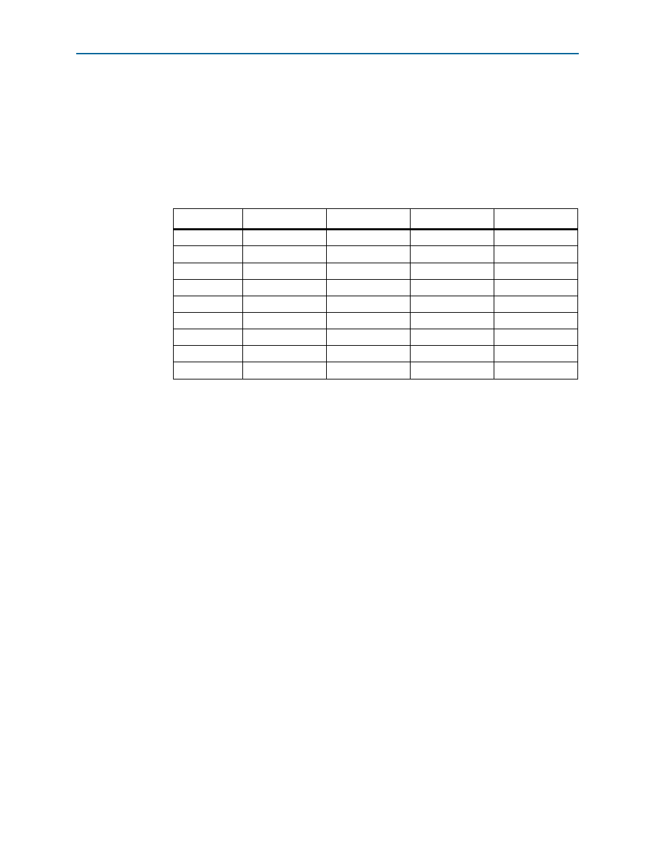
outlines the frequency requirements for core_clk and core_clk_out to meet
PCI Express link bandwidth constraints. These requirements apply to IP Compiler for
PCI Express variations generated with all three design flows.
The frequencies and widths specified in
operation. If, after the mode is configured, auto negotiation results in a lesser link
width, the IP Compiler for PCI Express maintains the core_clk_out frequency of the
original setting. If auto negotiation results in a change from Gen2 to Gen1, the IP
Compiler for PCI Express maintains the core_clk_out frequency of the original
setting. In all cases the IP Compiler for PCI Express also maintains the original
datapath width.
pld_clk
The application layer and part of the adapter use this clock. Ideally, the pld_clk drives
all user logic within the application layer, including other instances of the IP Compiler
for PCI Express and memory interfaces. The pld_clk input clock pin is typically
connected to the core_clk_out output clock pin.
Avalon-ST Interface—Soft IP Implementation
The soft IP implementation of the IP Compiler for PCI Express uses one of several
possible clocking configurations, depending on the PHY (external PHY, Arria GX,
Arria II GX, Cyclone IV GX, HardCopy IV GX, Stratix II GX, or Stratix IV GX) and the
reference clock frequency. There are two clock input signals: refclk and either
clk125_in
for x1 or ×4 variations or clk250_in for ×8 variations.
The ×1 and ×4 IP cores also have an output clock, clk125_out, that is a 125 MHz
transceiver clock. For external PHY variations clk125_out is driven from the refclk
input. The ×8 IP core has an output clock, clk250_out, that is the 250 MHz transceiver
clock output.
Table 7–1. core_clk_out Values for All Parameterizations
Link Width
Max Link Rate
Avalon-ST Width
core_clk
core_clk_out
×1
Gen1 64
125
MHz
125
MHz
×1
Gen1
64
62.5 MHz
62.5 MHz
×4
Gen1 64
125
MHz
125
MHz
×8
Gen1 64
250
MHz
250
MHz
×8
Gen1
128
250 MHz
125 MHz
×1
Gen2
64
125 MHz
125 MHz
×4
Gen2
64
250 MHz
250 MHz
×4
Gen2
128
250 MHz
125 MHz
×8
Gen2
128
500 MHz
250 MHz
Note to
:
(1) This mode saves power.