Design example bar/address map – Altera IP Compiler for PCI Express User Manual
Page 245
Chapter 15: Testbench and Design Example
15–13
Chaining DMA Design Example
August 2014
Altera Corporation
IP Compiler for PCI Express User Guide
■
altpcierd_cdma_tx_ecrc_64.v
, altpcierd_cdma_tx_ecrc_64_altcrc.v,
altpcierd_cdma_tx_ecrc_64.vo
—These modules contain the CRC32 generation
megafunction used in the altpcierd_ecrc_gen module. The .v files are used for
synthesis. The .vo file is used for simulation.
■
altpcierd_tx_ecrc_data_fifo
, altpcierd_tx_ecrc_ctl_fifo,
altpcierd_tx_ecrc_fifo
—These are FIFOs that are used in the ECRC generator
modules in altpcierd_cdma_ecrc_gen.
■
altpcierd_pcie_reconfig
—This module is instantiated when the PCIE reconfig
option on the System Settings page is turned on. It consists of a Avalon-MM
master which drives the PCIE reconfig Avalon-MM slave of the device under
test. The module performs the following sequence using the Avalon-MM
interface prior to any IP Compiler for PCI Express configuration sequence:
a. Turns on PCIE reconfig mode and resets the reconfiguration circuitry in the
hard IP implementation by writing 0x2 to PCIE reconfig address 0x0 and
asserting the reset signal, npor.
b. Reads the PCIE vendor ID register at PCIE reconfig address 0x89.
c. Increments the vendor ID register by one and writes it back to PCIE reconfig
address 0x89.
d. Removes the hard IP reconfiguration circuitry and SERDES from the reset state
by deasserting npor.
■
altpcierd_cplerr_lmi
—This module transfers the err_desc_func0 from the
application to the PCE Express hard IP using the LMI interface. It also retimes
the cpl_err bits from the application to the hard IP. This module is only used
with the hard IP implementation of the IP core.
■
altpcierd_tl_cfg_sample
—This module demultiplexes the configuration space
signals from the tl_cfg_ctl bus from the hard IP and synchronizes this
information, along with the tl_cfg_sts bus to the user clock (pld_clk)
domain. This module is only used with the hard IP implementation.
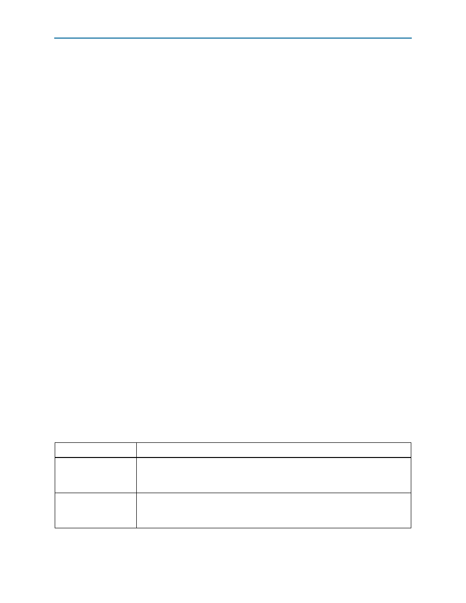
Design Example BAR/Address Map
The design example maps received memory transactions to either the target memory
block or the control register block based on which BAR the transaction matches. There
are multiple BARs that map to each of these blocks to maximize interoperability with
different variation files.
shows the mapping.
Table 15–4. Design Example BAR Map
Memory BAR
Mapping
32-bit BAR0
32-bit BAR1
64-bit BAR1:0
Maps to 32 KByte target memory block. Use the rc_slave module to bypass the chaining DMA.
32-bit BAR2
32-bit BAR3
64-bit BAR3:2
Maps to DMA Read and DMA write control and status registers, a minimum of 256 bytes.