Altera IP Compiler for PCI Express User Manual
Page 173
Chapter 7: Reset and Clocks
7–9
Clocks
August 2014
Altera Corporation
IP Compiler for PCI Express User Guide
Refer to
for this clocking configuration.
100 MHz Reference Clock and 250 MHz Application Clock
When a ×8 variation is configured on a HardCopy IV GX, Stratix II GX PHY, or
Stratix IV GX device, the 100 MHz clock is connected directly to the transceiver. The
clk250_out
is driven by the output of the transceiver.
The clk250_out must be connected to the clk250_in input, possibly through a clock
distribution circuit needed in the specific application. The user application interface is
synchronous to the clk250_in input.
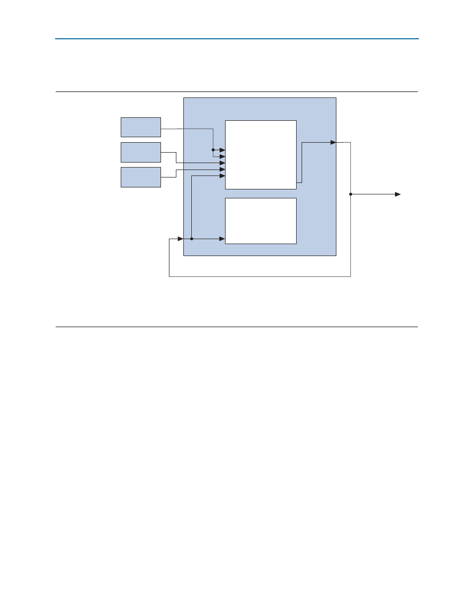
Figure 7–6. Arria GX, Arria II GX, Stratix II GX, or Stratix IV GX PHY ×1 or ×4 and Cyclone IV GX ×1 with 100 MHz
Reference Clock
Note to
(1) Different device families require different frequency ranges for the calibration and reconfiguration clocks. To determine the frequency range for
your device, refer to one of the following device handbooks:
Transceiver Architecture
in Volume II of the Arria II Device Handbook,
in Volume 2 of the Cyclone IV Device Handbook, or
Volume 2 of the Stratix IV Device Handbook.
(2) Refer to
for information about the core_clk_out frequencies for different device families and variations.
refclk
clk62.5_out
or
clk125_out
Application Clock
pld_clk
tx_clk_out
<variant>_serdes.v or .vhd
(ALTGX or ALT2GX
Megafunction)
<variant>.v or .vhd
<variant>_core.v or .vhd
(PCIe MegaCore Function)
rx_cruclk
pll_inclk
cal_blk_clk
reconfig_clk
fixedclk
100-MHz
Clock Source
Calibration
Clock Source
Reconfig
Clock Source
Note (1)
(2)