Multiple wait states throttle data transmission – Altera IP Compiler for PCI Express User Manual
Page 341
Chapter :
B–23
Descriptor/Data Interface
August 2014
Altera Corporation
IP Compiler for PCI Express User Guide
In clock cycle five, the second transaction layer packet is not immediately
acknowledged because of additional overhead associated with a 64-bit address, such
as a separate number and an LCRC. This situation leads to an extra clock cycle
between two consecutive transaction layer packets.
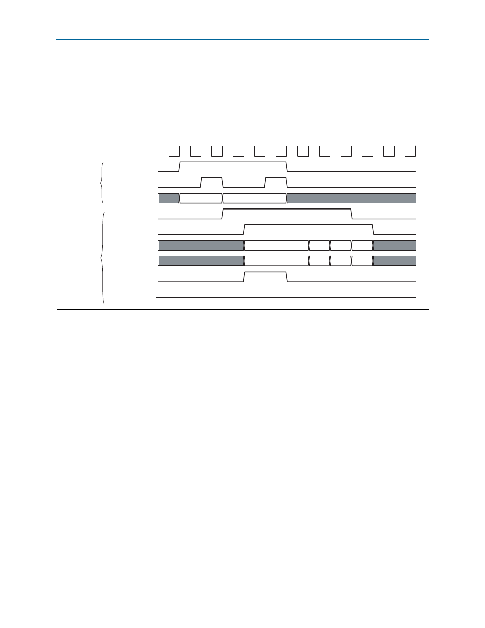
Multiple Wait States Throttle Data Transmission
In this example, the application transmits a 32-bit memory write transaction. Address
bit 2 is set to 0. Refer to
. No wait states are inserted during the first two
data phases because the IP core implements a small buffer to give maximum
performance during transmission of back-to-back transaction layer packets.
Figure B–20. TX 64-Bit Memory Read Request Waveform
clk
tx_req
tx_ack
tx_desc[127:0]
tx_dfr
tx_dv
tx_data[63:32]
tx_data[31:0]
tx_ws
tx_err
MEMRD64
MEMWR64
DW 1
DW 3
DW 5
DW 7
DW 0
DW 2
DW 4
DW 6
1
2
3
4
5
6
7
8
9
10
11
12
Descriptor
Signals
Data
Signals