Altera IP Compiler for PCI Express User Manual
Page 27
Chapter 2: Getting Started
2–11
Viewing the Generated Files
August 2014
Altera Corporation
IP Compiler for PCI Express User Guide
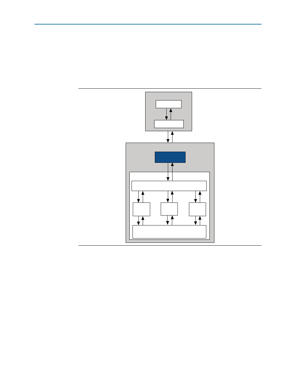
illustrates the top-level modules of this design. As this figure illustrates,
the IP Compiler for PCI Express connects to a basic root port bus functional model
(BFM) and an application layer high-performance DMA engine. These two modules,
when combined with the IP Compiler for PCI Express, comprise the complete
example design. The test stimulus is contained in altpcietb_bfm_driver_chaining.v.
The script to run the tests is runtb.do. For a detailed explanation of this example
design, refer to
Chapter 15, Testbench and Design Example
.
f
The design files used in this design example are the same files that are used for the
. You can download the required
files on the
product page. This
product page includes design files for various devices. The example in this document
uses the Stratix IV GX files. You can generate, simulate, and compile the design
example with the files and capabilities provided in your Quartus II software and IP
installation. However, to configure the example on a device, you must also download
altpcie_demo.zip,
which includes a software driver that the example design uses,
fr
Figure 2–6. Testbench for the Chaining DMA Design Example
Endpoint Example
Root Port Driver
x8 Root Port Model
Root Port BFM
IP Compiler
for PCI Express
PCI Express Link
Endpoint Application
Layer Example
DMA
Write
RC
Slave
(Optional)
Endpoint
Memory
(32 KBytes)
Traffic Control/Virtual Channel Mapping
Request/Completion Routing
DMA
Read