Altera IP Compiler for PCI Express User Manual
Page 240
15–8
Chapter 15: Testbench and Design Example
Chaining DMA Design Example
IP Compiler for PCI Express User Guide
August 2014
Altera Corporation
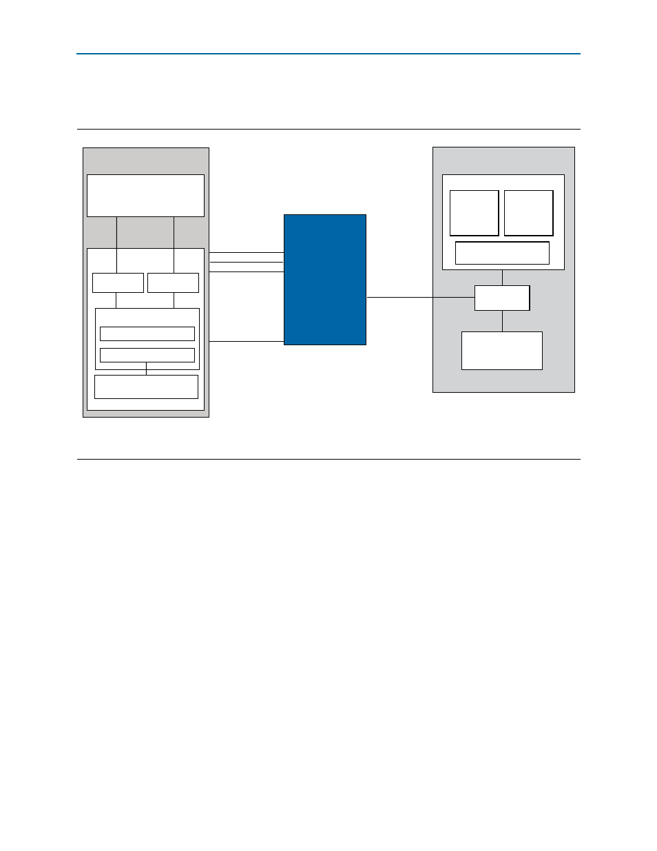
shows a block diagram of the design example connected to an external
RC CPU.
The block diagram contains the following elements:
■
Endpoint DMA write and read requester modules.
■
The chaining DMA design example connects to the Avalon-ST interface of the IP
Compiler for PCI Express when in Avalon-ST mode, or to the ICM when in
descriptor/data mode. (Refer to
Appendix C, Incremental Compile Module for
Descriptor/Data Examples
). The connections consist of the following interfaces:
■
The Avalon-ST RX receives TLP header and data information from the IP
Compiler for PCI Express
■
The Avalon-ST TX transmits TLP header and data information to the IP
Compiler for PCI Express
■
The Avalon-ST MSI port requests MSI interrupts from the IP Compiler for PCI
Express
■
The sideband signal bus carries static information such as configuration
information
■
The descriptor tables of the DMA read and the DMA write are located in the BFM
shared memory.
■
A RC CPU and associated PCI Express PHY link to the endpoint design example,
using a root port and a north/south bridge.
Figure 15–3. Top-Level Chaining DMA Example for Simulation
Note to
(1) For a description of the DMA write and read registers, refer to
.
Root Complex
CPU
Root Port
Memory
Write
Descriptor
Table
Data
Chaining DMA
Endpoint Memory
Avalon-MM
interfaces
IP Compiler
for PCI Express
DMA Control/Status Register
DMA Read
Avalon-ST
Configuration
PCI Express
DMA Write
DMA Wr Cntl (0x0-4)
DMA Rd Cntl (0x10-1C)
RC Slave
Read
Descriptor
Table