Bit sdr mode – Altera IP Compiler for PCI Express User Manual
Page 225
Chapter 14: External PHYs
14–5
External PHY Support
August 2014
Altera Corporation
IP Compiler for PCI Express User Guide
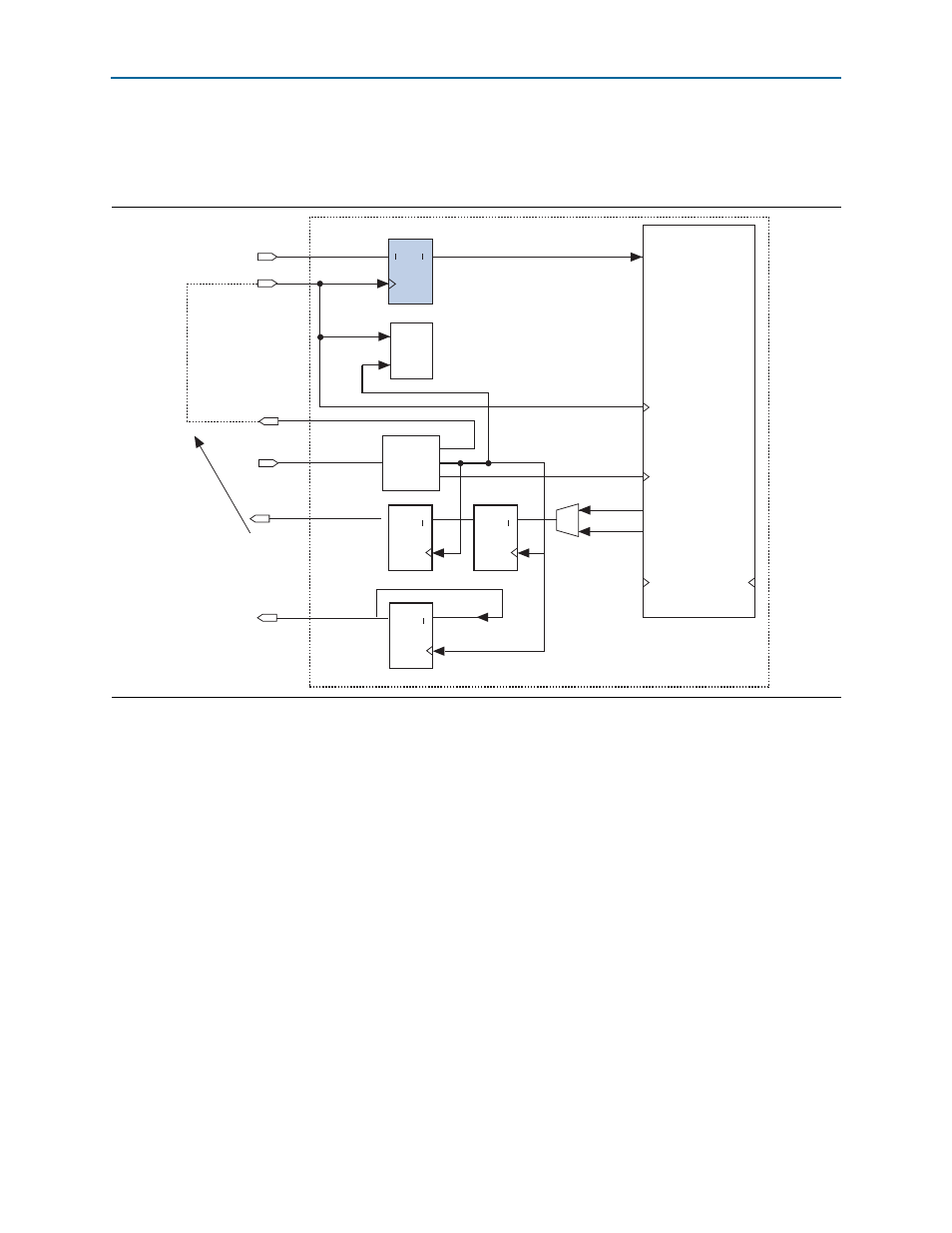
An edge detect circuit detects the relationships between the 125 MHz clock and the
250 MHz rising edge to properly sequence the 16-bit data into the 8-bit output
register.
8-bit SDR Mode
illustrates the implementation of the 8-bit SDR mode. This mode is
included in the file <variation name>.v or <variation name>.vhd and includes a PLL.
refclk
(pclk from the external PHY) drives the PLL inclock. The PLL has the
following outputs:
■
A 125 MHz output derived from the 250 MHz refclk used as the clk125_in for
the core and also to transition the incoming 8-bit data into a 16-bit register for the
rest of the logic.
■
A 250 MHz early output that is skewed early in relation to the refclk that is used to
clock an 8-bit SDR transmit data output register. The early clock PLL output clocks
the transmit data output register. The early clock is required to meet the specified
clock-to-out times for the common clock. You may need to adjust the phase shift
for your specific PHY and board delays. To alter the phase shift, copy the PLL
source file referenced in your variation file from the
Figure 14–4. 8-bit DDR Mode with a Source Synchronous Transmit Clock
IP Compiler
for PCI Express
clk125_in
tlp_clk
refclk
clk125_out
ENB
A
D
Q
1
Q
4
refclk (pclk)
rxdata
clk125_out
clk125_in
ENB
Q
Q
A
1
D
4
txdata
DDIO
Mode 3
PLL
ENB
Q
Q
A
1
D
4
txdata_h
txdata_l
Edge
Detect
& Sync
clk250_early
tlp_clk
External connection
in user logic
ENB
Q
Q
A
1
D
4
txclk