Altera IP Compiler for PCI Express User Manual
Page 174
7–10
Chapter 7: Reset and Clocks
Clocks
IP Compiler for PCI Express User Guide
August 2014
Altera Corporation
Refer to
for this clocking configuration.
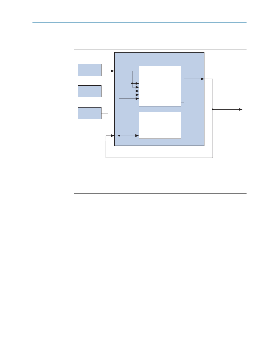
Figure 7–7. HardCopy IV GX, Stratix II GX, or Stratix IV GX ×8 with 100 MHz Reference Clock
Notes to
:
(1) Different device families require different frequency ranges for the calibration and reconfiguration clocks. To
determine the frequency range for your device, refer to one of the following device handbooks:
Transceiver
Architecture
in Volume II of the Arria II Device Handbook,
in Volume 2 of the Cyclone IV Device
Handbook, or
in Volume 2 of the Stratix IV Device Handbook.
(2) You must provide divide-by-two logic to create a 125 MHz clock source for fixedclk.
refclk
clk250_out
Application Clock
clk250_in
pld_clk
core_clk_out
<variant>
_serdes.v or .vhd
(ALTGX or ALT2GX
Megafunction)
<variant>.v or .vhd
<variant>
_core.v or .vhd
(PCIe MegaCore Function)
rx_cruclk
pll_inclk
cal_blk_clk
reconfig_clk
fixed_clk
refclk
100-MHz
Clock Source
Calibration
Clock Source
Reconfig
Clock Source
1/2
Note (2)
Note (1)