Tutorial: pci express 8gt, Methodology, Tutorial: pci express 8gt -1 – Altera JNEye User Manual
Page 152: Methodology -1
Tutorial: PCI Express 8GT
3
2015.05.04
UG-1146
This tutorial uses JNEye to run a link simulation. This example and its associated channel models are
provided with the JNEye distribution. The configuration file Demo.jne (included in the software distribu‐
tion) contains the same link topology and a majority of the link settings discussed in this tutorial.
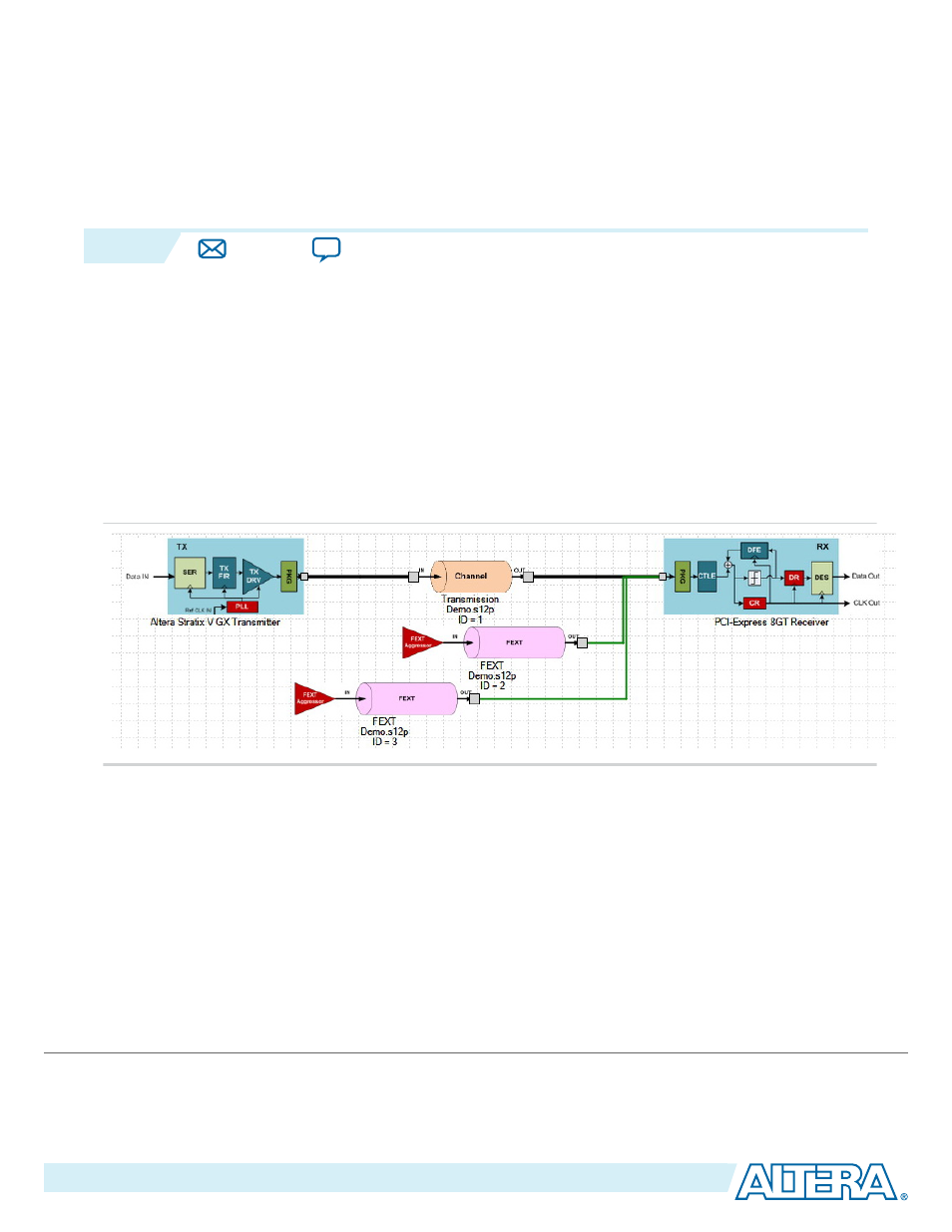
In this tutorial, a link that approximates a typical PCI-Express 8GT system with an Altera Stratix V GX
transmitter and a generic PCI-Express 8GT receiver is built and simulated in JNEye. The following figure
shows the link topology.
Note: This link configuration and simulation are for demonstration purposes. It is not intended for
actual implementation. Consult Altera design guidelines for actual high-speed link design and
implementation.
Figure 3-1: Example of PCI-Express 8GT Link Topology
Related Information
The Link and Simulation Setting tab sets the global link parameters and simulation configurations.
Methodology
This simulation emulates an Altera Stratix V GX transmitter (with embedded package model), a PCI
Express 8GT receiver (with embedded package model), and a ~18-inch backplane channel. Per PCI
Express 8GT specifications, the link operates at 8 Gbps with a bit error rate (BER) < 10
–12
. The transmitter
must have a minimum differential output voltage of 800 mV and a rise/fall time of ~35 ps (at 0.8 V V
OD
).
In this simulation, the Stratix V GX transmitter is set to 800 mV V
OD
(VOD level = 40). Additionally, the
©
2015 Altera Corporation. All rights reserved. ALTERA, ARRIA, CYCLONE, ENPIRION, MAX, MEGACORE, NIOS, QUARTUS and STRATIX words and logos are
trademarks of Altera Corporation and registered in the U.S. Patent and Trademark Office and in other countries. All other words and logos identified as
trademarks or service marks are the property of their respective holders as described at
www.altera.com/common/legal.html
. Altera warrants performance
of its semiconductor products to current specifications in accordance with Altera's standard warranty, but reserves the right to make changes to any
products and services at any time without notice. Altera assumes no responsibility or liability arising out of the application or use of any information,
product, or service described herein except as expressly agreed to in writing by Altera. Altera customers are advised to obtain the latest version of device
specifications before relying on any published information and before placing orders for products or services.
www.altera.com
101 Innovation Drive, San Jose, CA 95134