Altera JNEye User Manual
Page 173
Advertising
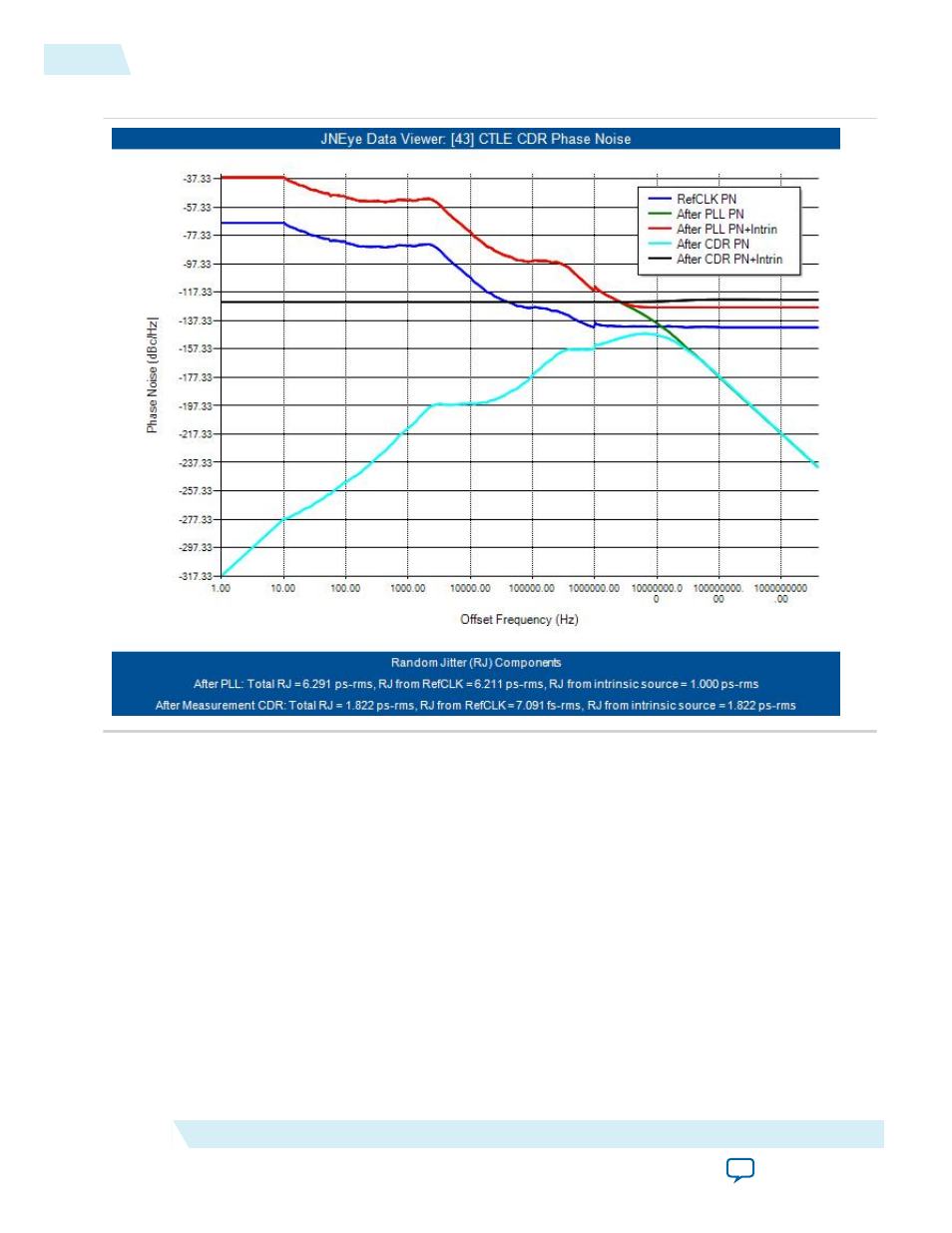
Figure 3-22: Phase Noise of Reference Clock and Its Transitions through PLL and CDR
At the output of the PCI-Express 8G receiver’s 1-Tap DFE, the following figures show that the DFE has
further opened the eye diagram with a total jitter of 1 UI (at BER < 10
-12
, with ideal clock and sinusoidal
jitter from the transmitter reference clock) and 0.53 UI (with CDR recovered clock) and eye diagram
opening height of 0 mV (with ideal clock) and 66 mV (with recovered clock). The BER bathtub curve and
contour show good behavior and successfully meet the PCI-Express 8GT RX requirements (TJ < 0.7 UI
and eye diagram height > 25 mV; refer to PCI-Express Base Specification 4.3).
3-22
Analysis
UG-1146
2015.05.04
Altera Corporation
Tutorial: PCI Express 8GT
Advertising
See also other documents in the category Altera Measuring instruments:
- MAX 10 JTAG (15 pages)
- MAX 10 Power (21 pages)
- Unique Chip ID (12 pages)
- Remote Update IP Core (43 pages)
- Device-Specific Power Delivery Network (28 pages)
- Device-Specific Power Delivery Network (32 pages)
- Hybrid Memory Cube Controller (69 pages)
- ALTDQ_DQS IP (117 pages)
- MAX 10 Embedded Memory (71 pages)
- MAX 10 Embedded Multipliers (37 pages)
- MAX 10 Clocking and PLL (86 pages)
- MAX 10 FPGA (26 pages)
- MAX 10 FPGA (56 pages)
- USB-Blaster II (22 pages)
- GPIO (22 pages)
- LVDS SERDES (27 pages)
- User Flash Memory (33 pages)
- ALTDQ_DQS2 (100 pages)
- Avalon Tri-State Conduit Components (18 pages)
- Cyclone V Avalon-MM (166 pages)
- Cyclone III FPGA Starter Kit (36 pages)
- Cyclone V Avalon-ST (248 pages)
- Stratix V Avalon-ST (286 pages)
- Stratix V Avalon-ST (293 pages)
- DDR3 SDRAM High-Performance Controller and ALTMEMPHY IP (10 pages)
- Arria 10 Avalon-ST (275 pages)
- Avalon Verification IP Suite (224 pages)
- Avalon Verification IP Suite (178 pages)
- FFT MegaCore Function (50 pages)
- DDR2 SDRAM High-Performance Controllers and ALTMEMPHY IP (140 pages)
- Floating-Point (157 pages)
- Integer Arithmetic IP (157 pages)
- Embedded Peripherals IP (336 pages)
- JESD204B IP (158 pages)
- Low Latency Ethernet 10G MAC (109 pages)
- LVDS SERDES Transmitter / Receiver (72 pages)
- Nios II Embedded Evaluation Kit Cyclone III Edition (3 pages)
- Nios II Embedded Evaluation Kit Cyclone III Edition (80 pages)
- IP Compiler for PCI Express (372 pages)
- Parallel Flash Loader IP (57 pages)
- Nios II C2H Compiler (138 pages)
- RAM-Based Shift Register (26 pages)
- RAM Initializer (36 pages)
- Phase-Locked Loop Reconfiguration IP Core (51 pages)
- DCFIFO (28 pages)