Generating the example design testbench – Altera Stratix V Avalon-ST User Manual
Page 13
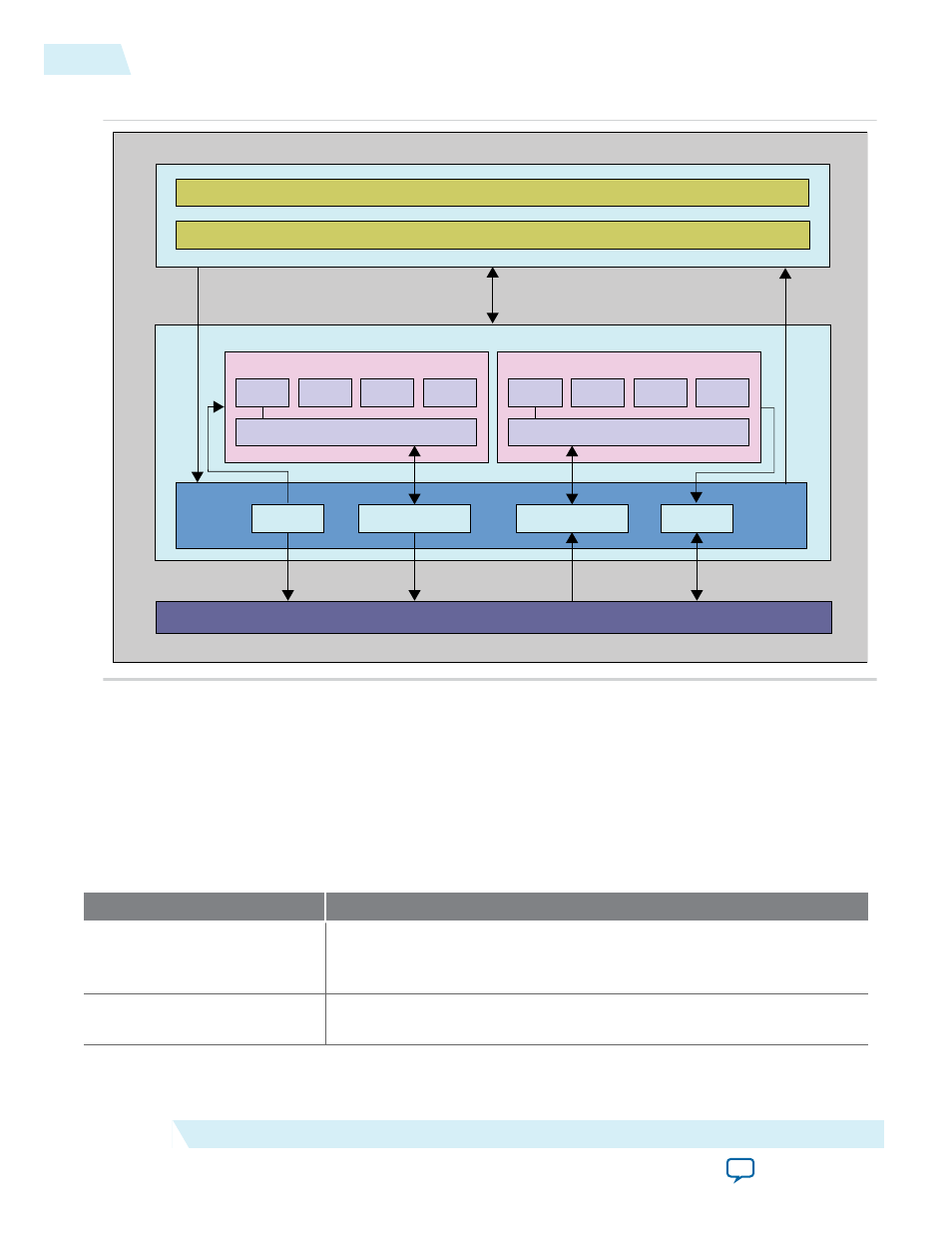
Figure 2-1: SR-IOV Example Design Block Diagram
Hard IP for PCI Express
SR-IOV Bridge
Rd_DC0
Rd_DC1
Rd_DC2
Rd_DC3
Read DMA Router
APPs - sriov_dma_app_g3x8_256b.qsys
sriov_top_dma_gen3_x8_256.qsys
rddc_ctl - rddc_ctl_256b.qsys
wrdc_ctl - wrdc_ctl_256b.qsys
Wr_DC0
Wr_DC1
Wr_DC2
Wr_DC3
Write DMA Router
User Application Logic (On-Chip Memories)
DMA Write
TX Slave
RX Master
DMA Read
Related Information
Generating the Example Design Testbench
Follow these steps to generate the SR-IOV DMA example design testbench:
1. Copy
<install_dir>/ ip/altera/altera_pcie/altera_pcie_sriov/example_design/sriov_top_dma_gen3_x8_256b.qsys
to your working directory. This top-level Qsys design includes three subsystems.
Qsys Subsystem
Description
sriov_dma_app_g3x8_
256b.qsys
This subsystem implements of the Read DMA read and Write DMA
modules and the Read and Write Descriptor Controllers. the DMA
engine.
rddc_ctl_256b.qsys
This subsystem implements the Read Descriptor Controller for 4 Read
DMA channels.
2-2
Generating the Example Design Testbench
UG-01097_sriov
2014.12.15
Altera Corporation
Getting Started with the SR-IOV DMA Example Design