Altera Stratix V Avalon-ST User Manual
Page 60
Signal
Direction
Description
pin_perst
Input
Active low reset from the PCIe reset pin of the device.
Refer to the appropriate Stratix V device pinout for correct pin
assignment for more detailed information about these pins. The
PCI Express Card Electromechanical Specification 2.0 specifies
this pin to require 3.3 V. You can drive this 3.3V signal to the
nPERST*
even if the V
VCCPGM
of the bank is not 3.3V if the
following 2 conditions are met:
• The input signal meets the V
IH
and V
IL
specification for
LVTTL.
• The input signal meets the overshoot specification for 100°C
operation as specified by the “Maximum Allowed Overshoot
and Undershoot Voltage” section in volume 3 of the Stratix V
Device Handbook.
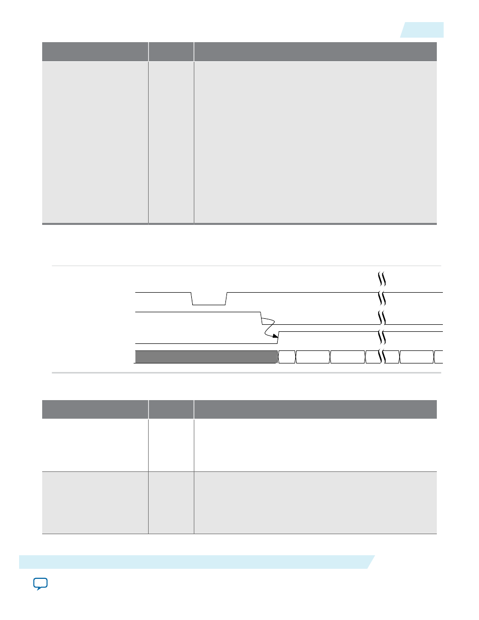
Figure 4-12: Reset and Link Training Timing Relationships
The following figure illustrates the timing relationship between
npor
and the LTSSM L0 state.
npor
IO_POF_Load
PCIe_LinkTraining_Enumeration
dl_ltssm[4:0]
detect detect.active polling.active
L0
Table 4-13: Hard IP Reset Status Signals
Signal
Direction
Description
pld_clk_inuse
Output
When asserted, indicates that the Hard IP Transaction Layer is
using the
pld_clk
as its clock and is ready for operation with the
Application Layer. For reliable operation, hold the Application
Layer in reset until
pld_clk_inuse
is asserted.
pld_core_ready
Input
When asserted, indicates that the Application Layer is ready for
operation and is providing a stable clock to the
pld_clk
input. If
the
coreclkout_hip
Hard IP output clock is sourcing the
pld_
clk
Hard IP input, this input can be connected to the
serdes_
pll_locked
output.
UG-01097_sriov
2014.12.15
Reset, Status, and Link Training Signals
4-25
Interfaces and Signal Descriptions
Altera Corporation