B5 pi function, Fig 5.13 pi block diagram, Programming 5 - 23 – Yaskawa E7L Drive Bypass User Manual
Page 115
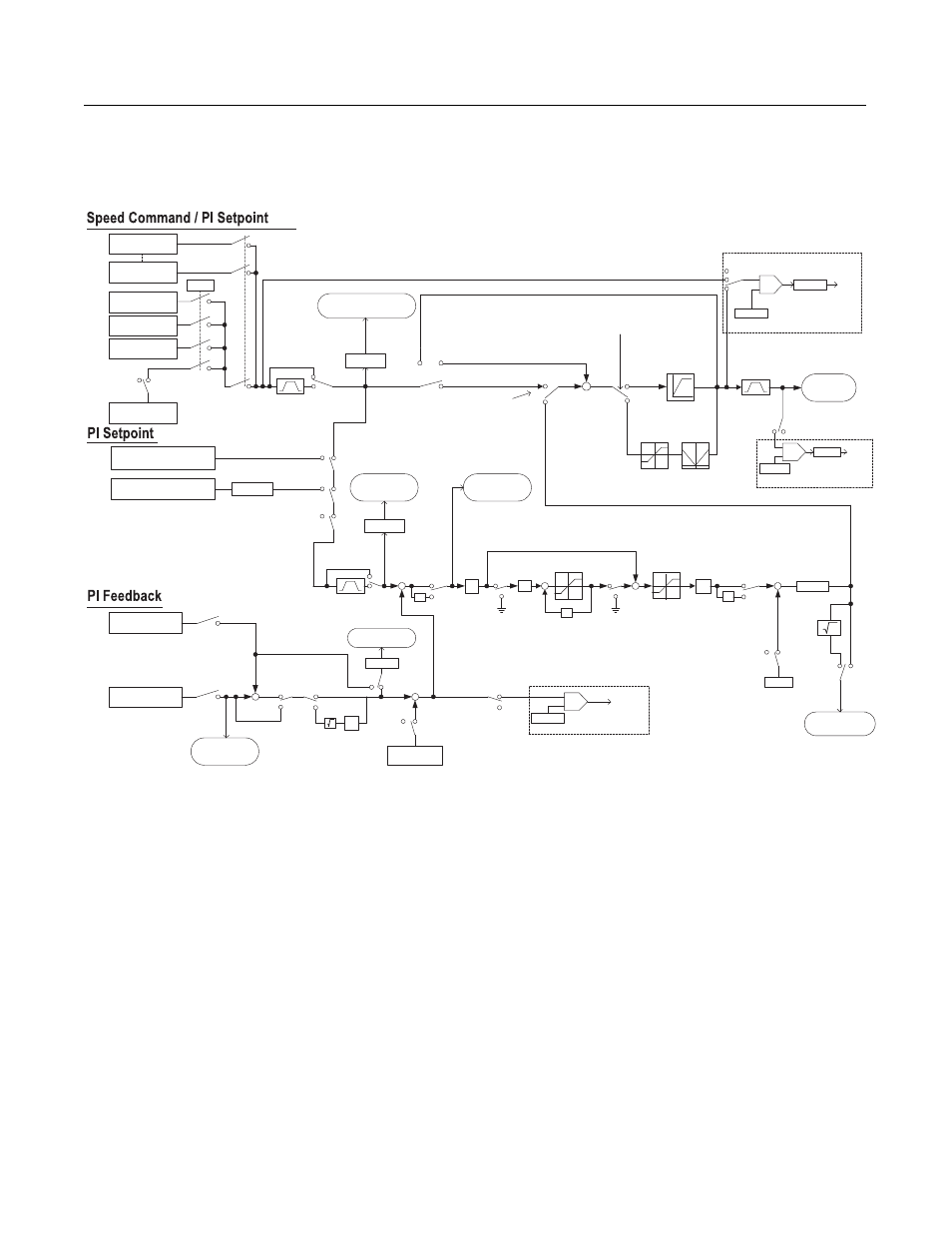
Programming 5 - 23
b5 PI Function
The capability to accept an analog signal as feedback for a PI (Proportional + Integral) control function is built into the Drive.
Fig 5.13 PI Block Diagram
Bypass units are shipped with the parameters in Table 5.1 and Table 5.2 pre-established for the configuration ordered.
To add PI control to a Bypass unit; observe the control options that are included in the unit by review of the model number on
the nameplate (inside of door and external lower right side) as well as the option codes and model number description in
Chapter 1. Then revise the parameter settings indicated in Table 5.3 and 5.4 for a line of data, in Table 5.4, with the same
(or similar) combination of options and sources for the speed and run commands. This will add the logic required for PI con-
trol to that required for Bypass control.
Table 5.3 includes parameters that are the same regardless of control options specified while Table 5.4 provides detail on the
option dependent parameters.
Option Card
Serial Com
Terminal A1
D1-01
D1-04
D1-02
Output
frequency
P
1/t
1/t
Z
-1
b1-01
1
2
3
Frequency Reference
using multi-step
command
Frequency reference
(U1-01)
PI Set Point
(U1-38)
Proportional
gain
b5-02
I-time
b5-03
I - limit
b5-04
PI Limit
b5-06
PI delay time
b5-08
PI offset
(b5-07)
+
+
+ +
PI output monitor
(U1-37)
b5-01=0
ON
PI control is OFF under the following
conditions:
- b5-01=0
- During JOG command input
- H3-xx=19 and the terminal status is
ON
Upper limit
Fmax x109%
+
+
b5-01=3
b5-01=1
Upper limit
Fmax x109%
Lower limit
Fmax x109%
Lower limit 0
4
MEMOBUS Reg. 06H
PI target value
Integral Hold
H1-xx=31
Integral Reset
H1-xx=30
PI Output
Characteristic
b5-09
b5-11
1
0
Enable / Disable reverse operation
when PI output is negative
Constant b5-19
b5-18
0
1
0
PI SFS
b5-17
PI SFS cancel
H1-xx=34
0
1
o1-03
Scaling
b5-20
Scaling
1
0
1
1
0
Reg. 0Fh, bit 1
Terminal A1
Terminal A2
PI Differential
Fdbk. H3-09=16
1
0
H3-09=B
1
0
1
0
PI Differential
Fdbk. H3-09=16
PI Differential
Fdbk. H3-09=16
Z
-1
1
0
1
0
PI Input
Caracteristic
H1-xx=35
1
0
Z
-1
PI SFS
b5-17
PI SFS cancel
H1-xx=34
0
1
b5-20
Scaling
PI Input
(U1-36)
+
-
PI Feedback 2
(U1-53)
0
1
PI Differential
Fdbk. H3-09=16
1
0
b5-28
PI Feedback
(U1-24)
b5-20
Scaling
1
0
1
0
b5-07
0
1
+
+
PI Differential
Fdbk. H3-09=16
-
+
+
+
+
-
b5-24
PI Wake Up Level
PI
Wake Up
PI Snooze Function
b5-10
0
1
b5-30
PI Output
Gain
PI offset
H3-09=16
+
-
b5-22
PI Snooze Level
PI
Snooze
PI Snooze Function
+
-
b5-15
Sleep Level
RUN
on/off
0
1
b5-16
Delay
Timer
Sleep Function
Sleep function
selection b5-21
SFS
OFF
b5-23
Delay
Timer
PI Differential
Fdbk. H3-09=16
2
2
0
o
r 1
0 or 1
2
Sleep function
selection b5-21
Sleep function
selection b5-21
P
b5-29
Characteristic
H1