Fig 6.1 electronic bypass control board layout, Diagnostic & troubleshooting 6 - 5 – Yaskawa E7L Drive Bypass User Manual
Page 177
Advertising
Diagnostic & Troubleshooting 6 - 5
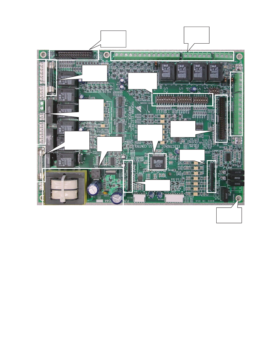
The overall layout of PCB A2 is shown in Figure 6.1 for further reference.
Fig 6.1 Electronic Bypass Control Board Layout
Customer
Connection
Terminals
Connector
For cable to
Keypad
Customer
120V
Circuit Fuse
Customer
Configuration
Switches
Connector
For cable to
Drive
CPLD
Logic
Processor
Option Port
Connector
Option Port
Connector
Connectors
to Panel
Wiring
Harnesses
Main
Control
Fuse
Power
Supply
Circuits
Mounting
Holes
5 Places
Advertising
This manual is related to the following products: