Internal bypass panel, Fig 1.7 internal bypass panel, Fig 1.8 pcb a2 control logic and connections – Yaskawa E7L Drive Bypass User Manual
Page 24
Advertising
Physical Installation 1 - 12
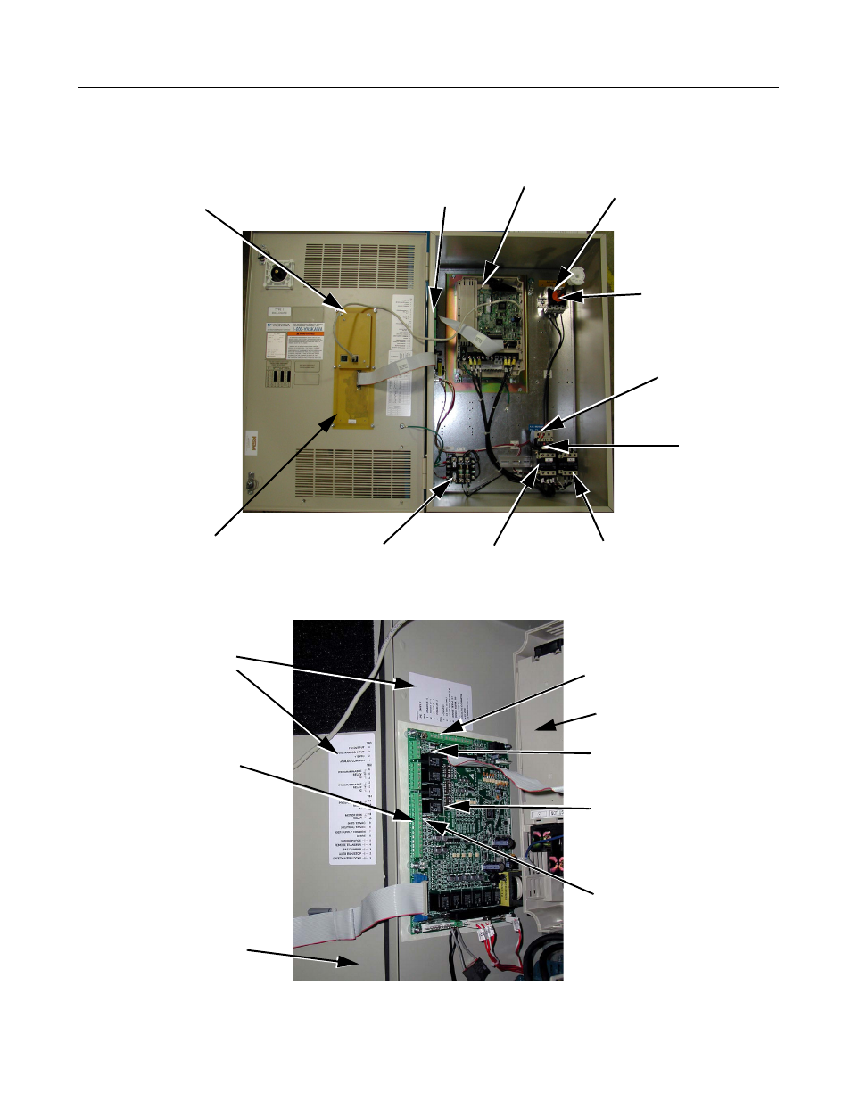
Internal Bypass Panel
Fig 1.7 Internal Bypass Panel
Fig 1.8 PCB A2 Control Logic and Connections
Control Wiring
Terminal Strips
Drive
Input
Overload
Drive Digital
Output
Bypass
Relay
Contactor
Contactor
PCB A3
Load
Connections
Line
Connections
TB4, TB5 and Terminal PE
Drive
Keypad
TB1 through TB5
Disconnect
Label Defining
Customer Control
Circuit Connection
Points
Jumpers J2 and J3,
Analog Output Signal Level
DIP Switches S1, S2, S3
and S4 for Field
Configuration of
Drive/Bypass Operation
TB1, TB2 and TB3
Jumper J1, Digital Input
Voltage Source Selection
Hinged Enclosure
Door
Control Power
Transformer
Advertising
This manual is related to the following products: