10 2 byte and 4 byte spi masters, 2 byte and 4 byte spi masters – BECKHOFF EtherCAT IP Core for Xilinx FPGAs v3.00k User Manual
Page 114
PDI Description
III-102
Slave Controller
– IP Core for Xilinx FPGAs
10.2.10 2 Byte and 4 Byte SPI Masters
Some SPI masters do not allow an arbitrary number of bytes per access, the number of bytes per
access must be a multiple of 2 or 4 (maybe even more). The SPI slave interface supports such
masters. The length of the data phase is in control of the master and can be set to the appropriate
length, the length of the address phase has to be extended. The address phase of a read access can
be set to a multiple of 2/4 by using the 3 byte address mode and a wait state byte. The address phase
of a write access can be enhanced to 4 bytes using 3 byte address mode and an additional address
extension byte (byte 2) according to Table 51.
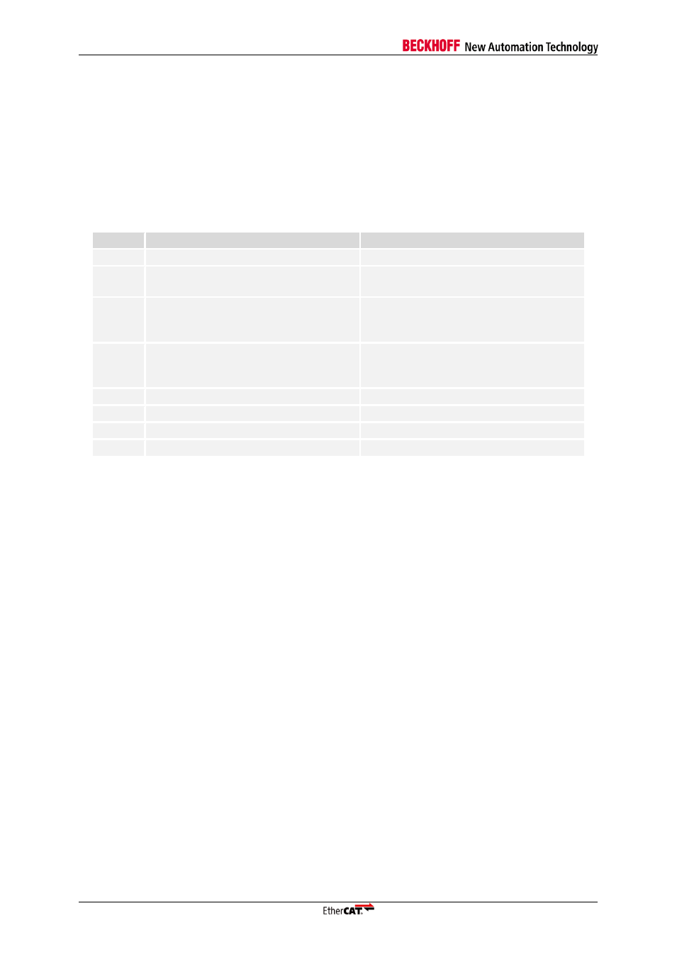
Table 51: Write access for 2 and 4 Byte SPI Masters
Byte
2 Byte SPI master
4 Byte SPI master
0
A[12:5]
address bits [12:5]
A[12:5]
address bits [12:5]
1
A[4:0]
address bits [4:0]
CMD0[2:0] write command: 100b
A[4:0]
address bits [4:0]
CMD0[2:0] 3 byte addressing: 110b
2
D0[7:0]
data byte 0
A[15:13]
address bits [15:13]
CMD1[2:0] 3 byte addressing: 110b
res[1:0]
two reserved bits, set to 00b
3
D1[7:0]
data byte 1
A[15:13]
address bits [15:13]
CMD2[2:0] write command: 100b
res[1:0]
two reserved bits, set to 00b
4
D2[7:0]
data byte 2
D0[7:0]
data byte 0
5
D3[7:0]
data byte 3
D1[7:0]
data byte 1
6
D4[7:0]
data byte 4
D2[7:0]
data byte 2
7
D5[7:0]
data byte 5
D3[7:0]
data byte 3
NOTE: The address phase of a write access can be further extended by an arbitrary number of address extension
bytes containing 110b as the command. The address phase of a read access can also be enhanced with
additional address extension bytes (the read wait state has to be maintained anyway). The address portion of the
last address extension byte is used for the access.