3 µcontroller access, 4 write access, 5 read access – BECKHOFF EtherCAT IP Core for Xilinx FPGAs v3.00k User Manual
Page 122: Μcontroller access, Write access, Read access, Table 55: 8 bit µcontroller interface access types
PDI Description
III-110
Slave Controller
– IP Core for Xilinx FPGAs
10.3.3 µController access
The 8 bit µController interface reads or writes 8 bit per access, the 16 bit µController interface
supports both 8 bit and 16 bit read/write accesses. For the 16 bit µController interface, the least
significant address bit together with Byte High Enable (BHE) are used to distinguish between 8 bit low
byte access, 8 bit high byte access and 16 bit access.
EtherCAT devices use Little Endian byte ordering.
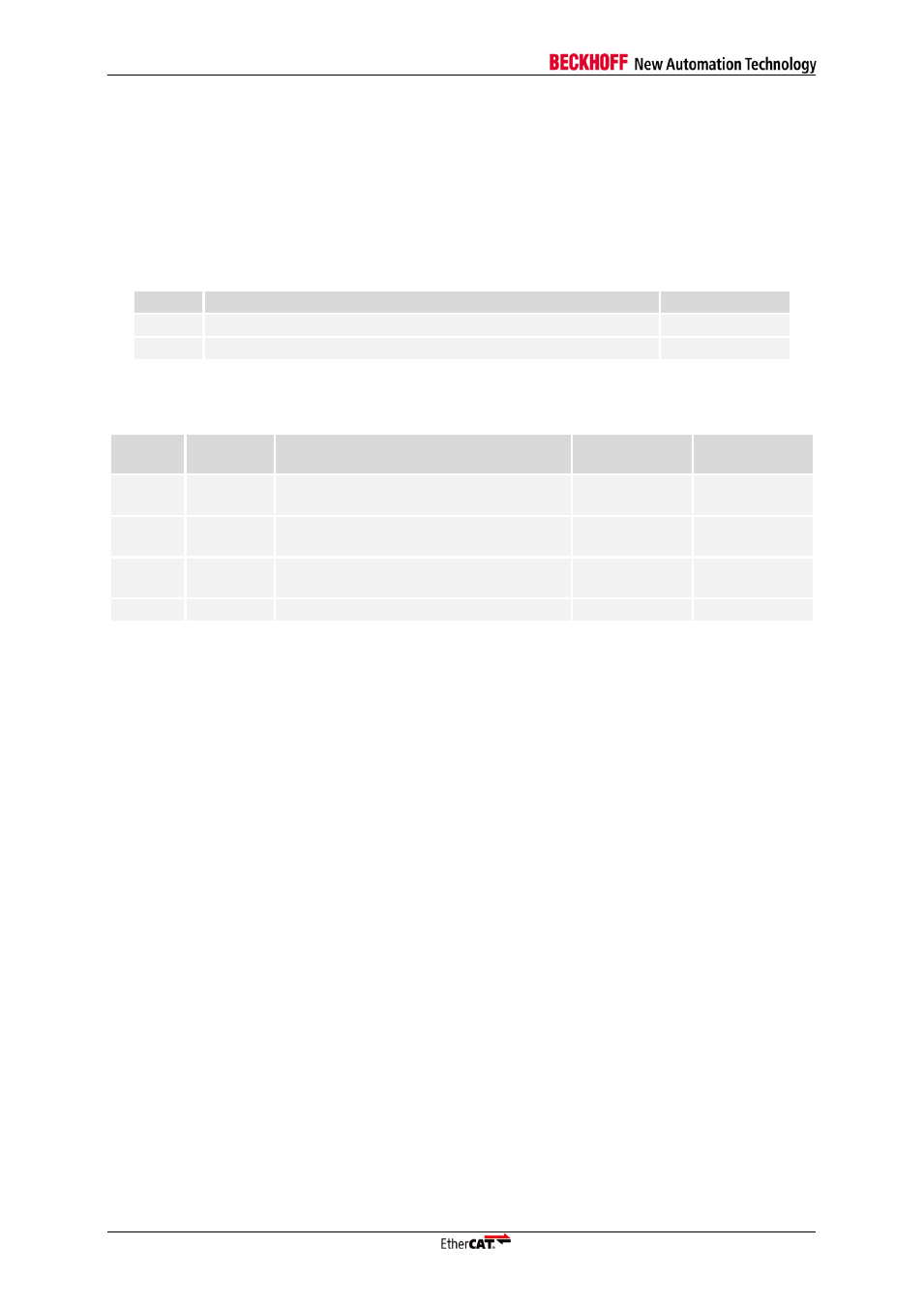
Table 55: 8 bit µController interface access types
ADR[0] Access
DATA[7:0]
0
8 bit access to ADR[15:0] (low byte, even address)
low byte
1
8 bit access to ADR[15:0] (high byte, odd address)
high byte
Table 56: 16 bit µController interface access types
ADR[0]
BHE
(act. low)
Access
DATA
[15:8]
DATA
[7:0]
0
0
16 bit access to ADR[15:0] and
ADR[15:0]+1 (low and high byte)
high byte
low byte
0
1
8 bit access to ADR[15:0]
(low byte, even address)
(RD only: copy
of low byte)
low byte
1
0
8 bit access to ADR[15:0]
(high byte, odd address)
high byte
(RD only: copy
of high byte)
1
1
invalid access
-
-
10.3.4 Write access
A write access starts with assertion of Chip Select (CS), if it is not permanently asserted. Address,
Byte High Enable and Write Data are asserted with the falling edge of WR (active low). Once the
µController interface is not BUSY, a rising edge on WR completes the µController access. A write
access can be terminated either by deassertion of WR (while CS remains asserted), or by deassertion
or CS (while WR remains asserted), or even by deassertion of WR and CS simultaneously. Shortly
after the rising edge of WR, the access can be finished by deasserting ADR, BHE and DATA. The
µController interface indicates its internal operation with the BUSY signal. Since the BUSY signal is
only driven while CS is asserted, the BUSY driver will be released after CS deassertion.
Depending on the configuration, the internal write access is either performed after the falling edge of
WR, or after the rising edge of WR. If the falling edge is selected, the internal write operation begins
with the falling edge of WR, and BUSY indicates when the write operation is finished. The internal
write operation is performed during the external write access.
If the rising edge of WR is selected, the internal operation begins with the rising edge of WR, i.e., after
the external write access. Thus, the external write access is very fast, but an access immediately
following will be delayed by the preceding write access. The maximum access time is higher in this
case.
10.3.5 Read access
A read access starts with assertion of Chip Select (CS), if it is not permanently asserted. Address and
BHE have to be valid before the falling edge of RD, which signals the start of the access. The
µController interface will show its BUSY state afterwards
– if it is not already busy executing a
preceding write access
– and release BUSY when the read data are valid. The read data will remain
valid until either ADR, BHE, RD or CS change. The data bus will be driven while CS and RD are
asserted. BUSY will be driven while CS is asserted.
With read busy delay configuration, BUSY deassertion for read accesses can be additionally delayed
for 15 ns, so external DATA setup requirements in respect to BUSY can be met.