1 clock source example schematics, Clock source example schematics, Figure 24: ethercat ip core clock source (mii) – BECKHOFF EtherCAT IP Core for Xilinx FPGAs v3.00k User Manual
Page 72: Figure 25: ethercat ip core clock source (rmii), Figure 26: ethercat ip core clock source (rgmii)
IP Core Signals
III-60
Slave Controller
– IP Core for Xilinx FPGAs
8.1.1
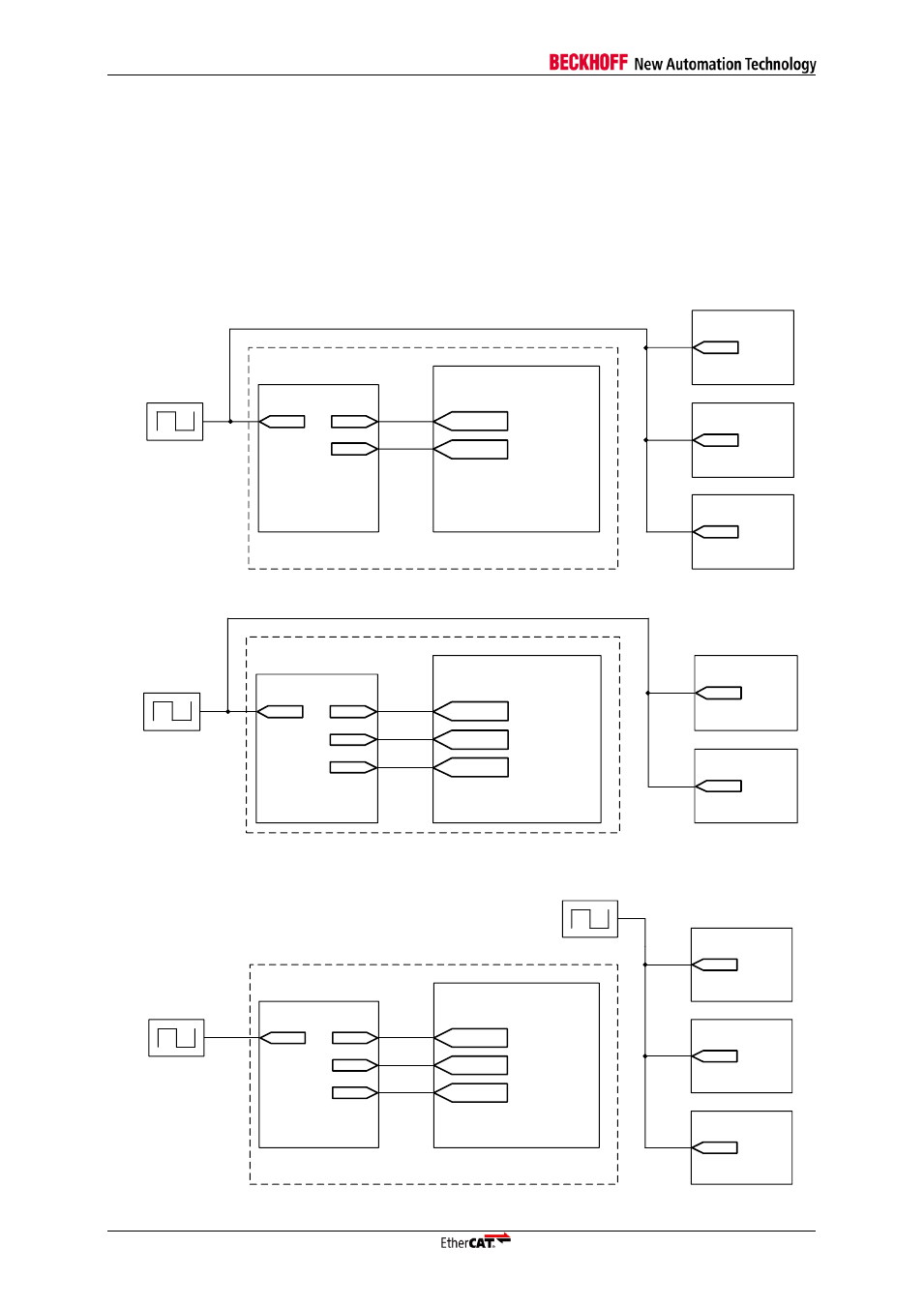
Clock source example schematics
The EtherCAT IP Core and the Ethernet PHYs have to share the same clock source. The initial
accuracy of the EtherCAT IP clock source has to be 25ppm or better.
Typically, the clock inputs of the EtherCAT IP Core (CLK25, CLK100, and optionally CLK50 or
CLK25_2NS) are sourced by a PLL inside the FPGA. The PLL has to use a configuration which
guarantees a fixed phase relation between clock input and clock outputs, in order to enable TX shift
compensation for the MII TX signals.
CLK25
EtherCAT IP Core
Ethernet
PHY
MII
CLK25
PLL
CLK_IN
CLK25
CLK100
CLK100
Ethernet
PHY
MII
CLK25
25 MHz
Ethernet
PHY
MII
CLK25
FPGA
Figure 24: EtherCAT IP Core clock source (MII)
CLK25
EtherCAT IP Core
Ethernet
PHY
RMII
REF_CLK
PLL
CLK_IN
CLK25
CLK100
CLK100
Ethernet
PHY
RMII
REF_CLK
50 MHz
CLK50
CLK50
FPGA
Figure 25: EtherCAT IP Core clock source (RMII)
CLK25
EtherCAT IP Core
Ethernet
PHY
RGMII
REF_CLK
PLL
CLK_IN
CLK25
CLK100
CLK100
Ethernet
PHY
RGMII
REF_CLK
25 MHz
Ethernet
PHY
RGMII
REF_CLK
FPGA
REF_CLK
CLK25_2NS
CLK25_2NS
Figure 26: EtherCAT IP Core clock source (RGMII)