BECKHOFF EtherCAT IP Core for Xilinx FPGAs v3.00k User Manual
Page 126
PDI Description
III-114
Slave Controller
– IP Core for Xilinx FPGAs
Parameter
Min
Max
Comment
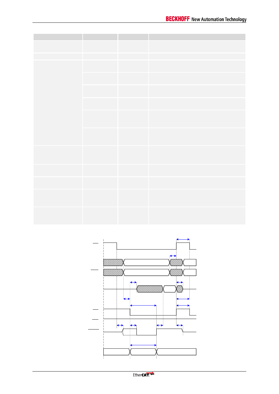
t
BUSY_to_WR_CS
WR or CS deassertion after BUSY
deassertion
t
WR_to_BUSY
BUSY assertion after WR deassertion
t
write
0 ns
External write time (WR assertion to BUSY
deassertion)
a) t
write_int
a) Configuration: write after falling edge of
WR (act. low)
b) t
write_int
-t
WR_delay
b) with preceding write access and t
WR_delay
< t
write_int
(Write after rising edge of WR)
c) 0 ns
c) without preceding write access or t
WR_delay
≥ t
write_int
(Write after rising edge of WR)
d) 95 ns
d) 8 bit access, absolute worst case with
preceding write access (t
WR_delay
= min,
t
WR_int
=max, Write after rising edge of WR)
e) 95 ns
e) 16 bit access, absolute worst case with
preceding write access (t
WR_delay
=min,
t
WR_int
=max, Write after rising edge of WR)
t
write_int
a) 55 ns
b) 55 ns
a) 95 ns
b) 95 ns
Internal write time
a) 8 bit access
b) 16 bit access
t
WR_delay
Delay between WR deassertion and
assertion
t
WR_to_RD
0 ns
Delay between WR deassertion and RD
assertion
t
CS_WR_overlap
Time both CS and WR have to be
deasserted simultaneously (only if CS is
deasserted at all)
t
CS_RD_overlap
Time both CS and RD have to be
deasserted simultaneously (only if CS is
deasserted at all)
t
CS_RD_to_DATA_release
BHE
t
ADR_BHE_setup
CS
BHE
RD
WR
DATA
BUSY
DATA
ADR
ADR
t
CS_to_BUSY
t
read
t
RD_to_BUSY
t
RD_delay
t
CS_delay
t
BUSY_to_DATA_valid
t
ADR_BHE_to_DATA_invalid
t
RD_to_DATA_driven
t
CS_to_BUSY_release
BHE
ADR
t
RD_CS_overlap
(with preceding write access)
Internal
state
Reading ADR
Idle
t
read_int
Idle
Figure 53: Read access (without preceding write access)