14 synthesis constraints, Synthesis constraints, Table 70: ethercat ip core constraints – BECKHOFF EtherCAT IP Core for Xilinx FPGAs v3.00k User Manual
Page 141
Synthesis Constraints
Slave Controller
– IP Core for Xilinx FPGAs
III-129
14 Synthesis Constraints
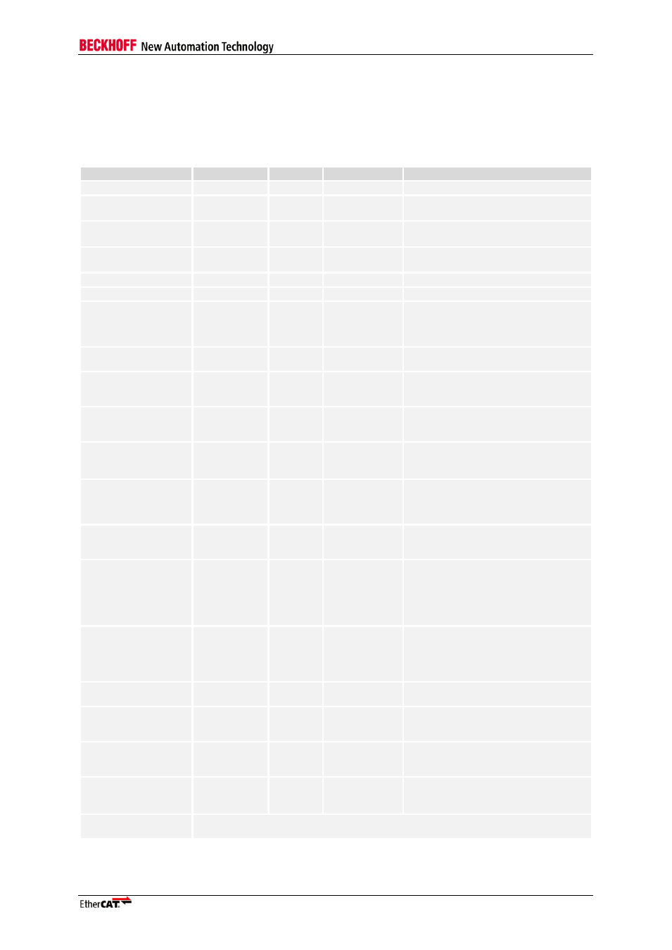
The following table contains basic IP Core constraints. Refer to Xilinx for details about RGMII
constraining.
Table 70: EtherCAT IP Core constraints
Signal
Requirement
Value
Clock reference
Description
CLK25
period
40 ns
Reference clock (25 MHz)
CLK25_2NS
a) period
b) phase shift
a) 40 ns
b) 2 ns
CLK25
Derived clock (25 MHz). Phase shift is rising
edge CLK25 to rising edge CLK25_2NS.
CLK50
a) period
b) phase shift
a) 20 ns
b) 0 ns
CLK25
Derived clock (50 MHz). Phase shift is rising
edge to rising edge.
CLK100
a) period
b) phase shift
a) 10 ns
b) 0 ns
CLK25
Derived clock (100 MHz). Phase shift is
rising edge to rising edge.
nRESET
Ignore timing
nRESET is asynchronous to any clock
MCLK
min. period
400 ns
IEEE802.3 requirement (2.5 MHz)
MDIO
a) setup
b) hold
at PHY input
a) 10 ns
b) 10 ns
MCLK
(rising edge)
MDIO is changed with falling edge of
MCLK, max. output skew of MCLK and
MDIO is 190 ns. Constraining is usually not
required. IEEE802.3 requirement.
MII_RX_CLK0-2
period
40 ns
MII receive reference clock (25 MHz).
IEEE802.3 requirement.
MII_RX_DATA0-2[3:0]
MII_RX_DV0-2
MII_RX_ERR0-2
a) setup
b) hold
a) 10 ns
b) 10 ns
MII_RX_CLK0-2
(rising edge)
IEEE802.3 requirement
MII_TX_CLK0-2
period
40 ns
MII transmit reference clock (25 MHz). Only
used for automatic TX Shift compensation.
IEEE802.3 requirement.
MII_TX_DATA0-2[3:0]
MII_TX_ENA0-2
Clock-to-Pin
a) min
b) max
a) 0 ns
b) 25 ns
TX_CLK0-2 from
PHY (rising
edge)
IEEE802.3 requirement
Clock-to-Pin
a) min
b) max
a) 0 ns
b) 10 ns
CLK25
(rising edge)
Incomplete alternative to IEEE802.3
requirement, keeps margin if TX Shift has
been determined and compensated. Refer
to section III for details.
PROM_CLK
period
App. dep.
I²C clock. Actual ESC output clock is
6.72 µs (
≈ 150 kHz). Min. 2.5µs (400 Khz)
for example I²C EEPROM chip.
PROM_DATA
a) setup
b) hold
a) 250 ns
b) 0 ns
PROM_CLK
a) rising edge
b) falling edge
PROM_DATA is changed in the middle of
the low phase of PROM_CLOCK, i.e., max.
output skew of PROM_CLK/PROM_DATA
is 1.43 µs. Constraining is usually not
required. Example I²C EEPROM chip
requirement.
RMII_RX_DATA0/1[1:0]
RMII_RX_DV0/1
RMII_RX_ERR0/1
RMII_TX_DATA0/1[1:0]
RMII_TX_ENA0/1
a) setup
b) hold
a) 4 ns
b) 2 ns
CLK50
(rising edge)
RMII specification requirement
RGMII_RX_CLK0-2
period
40 ns
RGMII receive reference clock (25 MHz).
RGMII spec. requirement.
RGMII_RX_CTL0-3
RGMII_RX_DATA0-
3[3:0]
a) setup
b) hold
a)
b)
RGMII_RX_CLK
0-2 (both edges)
Depending on RX_CLK delay option,
RGMII spec. requirement
RGMII_TX_CLK0-2
a) period
b) phase shift
a) 40 ns
b) 2 ns
CLK25_2NS
RGMII transmit reference clock (25 MHz),
derived from CLK25_2NS. RGMII spec.
requirement.
RGMII_TX_CTL0-3
RGMII_TX_DATA0-
3[3:0]
Clock-to-Pin
a) min
b) max
a)
b)
RGMII_TX_CLK
0-2 (both edges)
Depending on TX_CLK delay option,
RGMII spec. requirement
Other signals, especially
PDI signals
application dependent