Memory map, Memory map –2, Table 6–2 on – Altera RapidIO II MegaCore Function User Manual
Page 140
6–2
Chapter 6: Software Interface
Memory Map
RapidIO II MegaCore Function
August 2014
Altera Corporation
User Guide
Memory Map
lists the RapidIO II IP core memory map overview.
Detailed register descriptions for the CARs and CSRs are available in the RapidIO
Interconnect Specification v2.2. This user guide also includes the information in the
individual register descriptions, with the addition of the RapidIO II IP core default
values for the individual fields.
1
Bit numbering for register fields in the RapidIO II IP core is reversed from the bit
numbering in the register descriptions in the RapidIO Interconnect Specification v2.2.
Refer to
“Avalon-MM Interface Byte Ordering” on page 4–1
. The descriptions
provided in this user guide list the bit numbering in the RapidIO II IP core.
RW1C
Read/Write 1 to clear
UR0
Unused bits/read as 0
Table 6–1. Register Access Codes (Part 2 of 2)
Code
Description
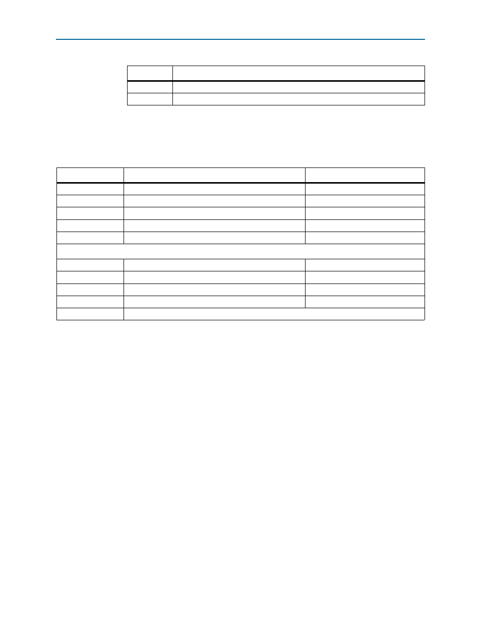
Table 6–2. RapidIO II IP Core Memory Map Ranges
Address Range
Name
Module
0x00–0x3C
Capability registers (CARs)
Standard registers
0x40–0x6F
Command and Status registers (CSRs)
Standard registers
0x100–0x15F
LP-Serial Extended Features block
Physical layer
0x200–0x27F
LP-Serial Lane Extended Features block
Physical layer
0x300–0x36F
Error Management Extensions Extended Features block
Standard registers
Implementation-Defined Space: 0x10080–0x107FF
0x10080–0x1029F
Maintenance module registers
Maintenance module
0x10300–0x103FC
I/O Logical layer Master module registers
I/O Logical layer Master module
0x10400–0x10510
I/O Logical layer Slave module registers
I/O Logical layer Slave module
0x10600–0x10624
Doorbell module registers
Doorbell module
0x10700–0x107FF
Reserved