Programmable logic decs-400 – Basler Electric DECS-400 User Manual
Page 192
180
9369700990 Rev R
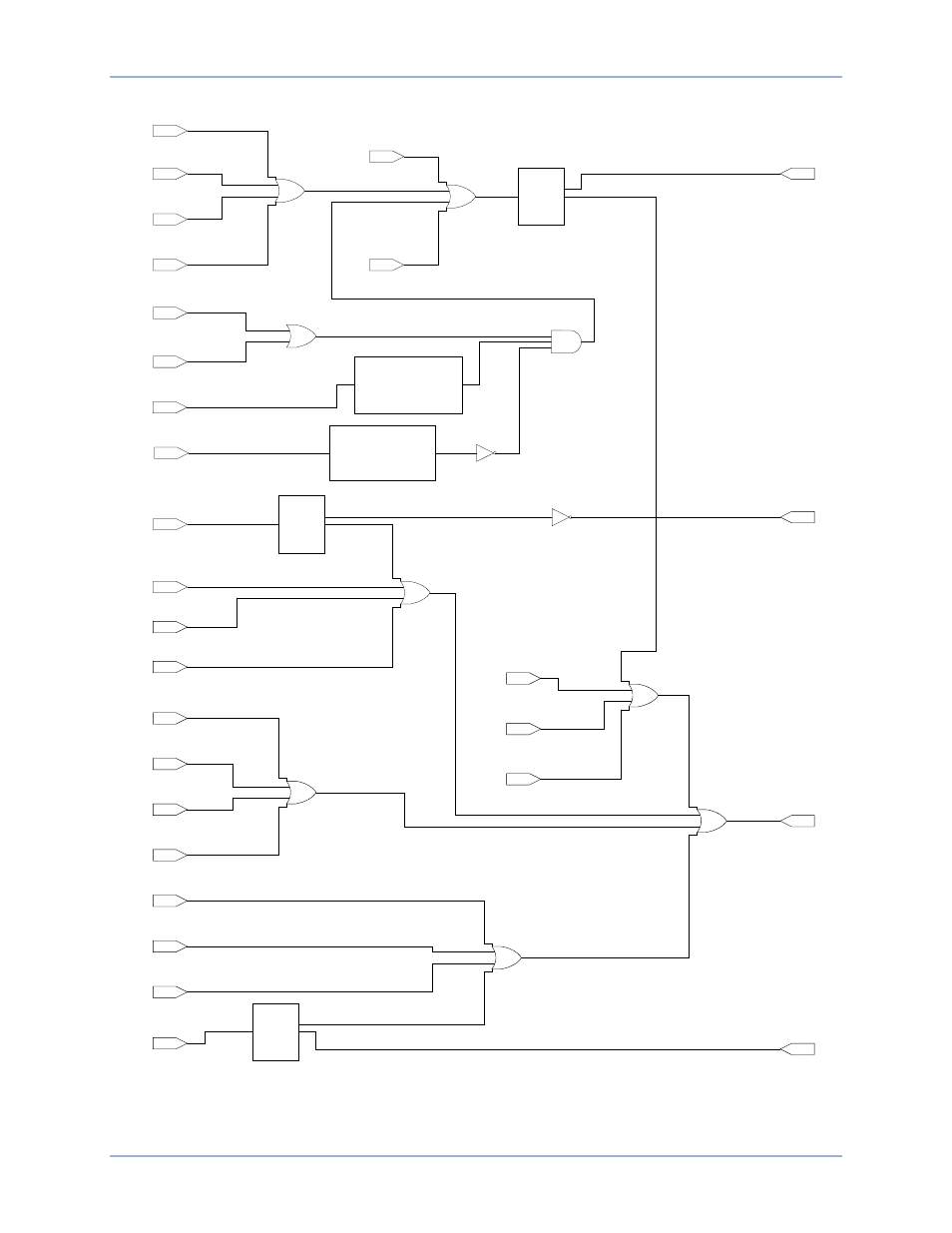
Figure 115. Dual DECS-400 With PSS (Part 3 of 3)
OEL Active
(Input Buffer)
Output Relay #3
Common Limiter(s)
(Output Buffer)
Transfer to FCR on
Loss of Sensing
Enable
(Output Buffer)
Relay Output #4
Field Overcurrent
(Output Buffer)
Layer 1
Gate 01
UEL Active
(Input Buffer)
SCL Active
(Input Buffer)
V/Hz Limiter Active
(Input Buffer)
Layer 1
Gate 02
Setpoint Adjustment
High Limit
(Input Buffer)
Setpoint Adjustment
Low Limit
(Input Buffer)
Underfrequency
Active
(Input Buffer)
u
2
u
3
u
4
u
1
x
1
MUX
u
4
u
4
Generator Overvoltage
Active
(Input Buffer)
Layer 1
Gate 05
Generator Undervoltage
Active
(Input Buffer)
Loss of Field
Active
(Input Buffer)
V/Hz Protection
Active
(Input Buffer)
Loss of
Isolation Module
Active
(Input Buffer)
Layer 1
Gate 04
Failed to Build Up
Active
(Input Buffer)
EDM Open Active
(Input Buffer)
EDM Shorted Active
(Input Buffer)
Field Overtemperature
Active
(Input Buffer)
Layer 1
Gate 06
Field Overvoltage
Active
(Input Buffer)
Loss of Sensing
Active
(Input Buffer)
u
2
u
3
u
4
u
1
x
1
MUX
u
4
u
4
Layer 1
Gate 04
u
2
u
3
u
4
u
1
x
1
MUX
u
4
u
4
Relay Output #2
Common Alarm
(Output Buffer)
Layer 2
Gate 02
Layer 2
Gate 03
Layer 1
Gate 03
Layer 1
Gate 04
Layer 1
Gate 03
PSS Voltage Limiter
Active
(Input Buffer)
Layer 2
Gate 01
PSS Voltage Unbalance
Active
(Input Buffer)
PSS Current Unbalance
Active
(Input Buffer)
PSS Speed Failure
Active
(Input Buffer)
Field Overcurrent
Active
(Input Buffer)
P0072-92
Unit Mode
(Input Buffer)
Soft Start
(Input Buffer)
Layer 4
Gate 04
Layer 1
Timer 1
Mode = Pickup/Dropout
T1 Time Delay = 10,000
T2 Time Delay = 0
Layer 2
Timer 1
Mode = Pickup/Dropout
T1 Time Delay = 0
T2 Time Delay = 10,000
Layer 3
Gate 03
Programmable Logic
DECS-400