Basler Electric DECS-400 User Manual
Page 197
9369700990 Rev R
185
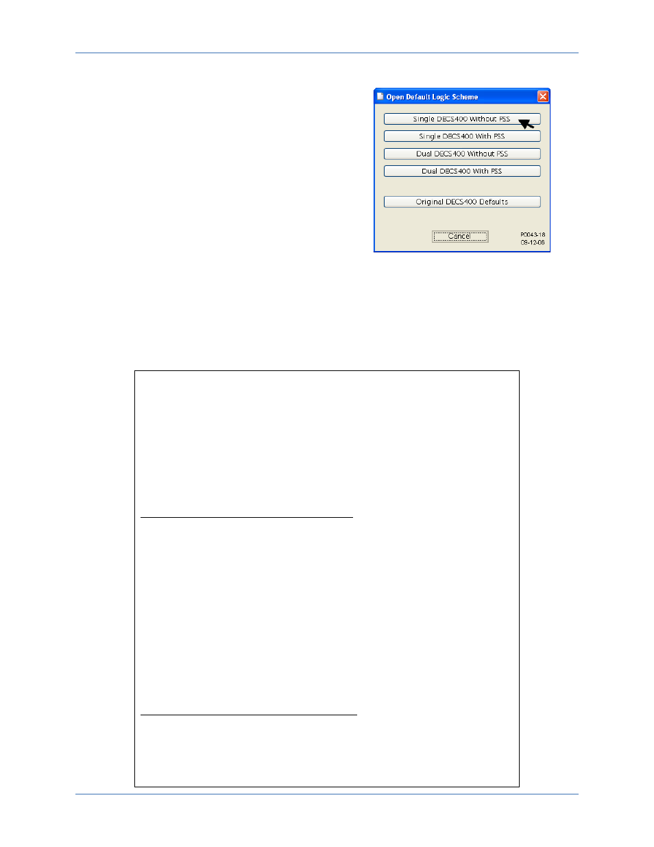
Open “Single DECS-400 Without PSS” Logic Scheme for Editing
1.
Open the “Single DECS-400 Without PSS”
logic scheme in BESTCOMS by clicking
File, Open Default Scheme…. When the
Open Default Logic Scheme window opens,
click the button labeled “Single DECS-400
Without PSS” (see Figure 120). Click the
Yes button in the warning dialog box to
continue opening the logic scheme. Once
the logic scheme has been opened, a
second dialog box will appear. Click the OK
button.
2.
Access the DECS Logic window by clicking
the Logic button on the BESTCOMS
toolbar.
3.
To view the active logic scheme (DECS
Logic Viewer), click the View Logic button in
the DECS Logic window.
Figure 120. Open Default Logic Scheme Window
Table 24 lists the logic associations of the modified “Single DECS-400 Without PSS” scheme. Lined out
entries in the list indicate logic associations that will be deleted. Bold entries in the list indicate logic
associations that will be added later in this example.
Table 24. Modified “Single DECS-400 Without PSS” Logic Scheme
{ SOURCE ---> DESTINATION }
=====> DESTINATION: Layer1
InputBuffer.Load Comp ---> Mux1.Input
InputBuffer.Contact Switch 5 ---> Mux2.Input
InputBuffer.Loss of Field Isolation Transducer ---> Mux3.Input
InputBuffer.Loss of Sensing ---> Mux4.Input
InputBuffer.Over Excitation Limit ---> Or1.Input1
InputBuffer.Under Excitation Limit ---> Or1.Input2
InputBuffer.Stator Current Limit ---> Or1.Input3
InputBuffer.Volts per Hz Limit ---> Or1.Input4
InputBuffer.Setpoint High Limit ---> Or2.Input1
InputBuffer.Setpoint Low Limit ---> Or2.Input2
Layer1.Or1.Output ---> Or3.Input2
Layer1.Or2.Output ---> Or3.Input3
InputBuffer.Under Freq Limit ---> Or3.Input4
Layer1.Mux3.Output2 ---> Or4.Input1
InputBuffer.Failed To Build Up ---> Or4.Input2
InputBuffer.EDM Open ---> Or4.Input3
InputBuffer.EDM Short ---> Or4.Input4
InputBuffer.Gen Over Voltage ---> Or5.Input1
InputBuffer.Gen Under Voltage ---> Or5.Input2
InputBuffer.Loss of Field ---> Or5.Input3
InputBuffer.Volts per Hz ---> Or5.Input4
InputBuffer.Field Over Temp ---> Or6.Input1
InputBuffer.Field Over Voltage ---> Or6.Input2
InputBuffer.Field Over Current ---> Or6.Input3
Layer1.Mux4.Output1 ---> Or6.Input4
InputBuffer.Contact Switch 10 ---> Not2.Input
Layer1.Mux1.Output2 ---> Not3.Input
Layer1.Mux3.Output1 ---> Not4.Input
DECS-400
Programmable Logic