Figure 3.1, 2 standard connection diagram, Drive regenerative unit – Yaskawa R1000 Series Power Regenerative Unit User Manual
Page 39: R1000
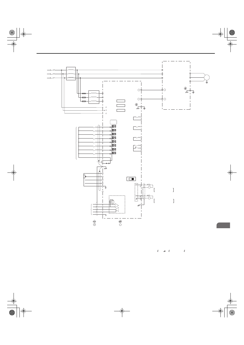
3.2 Standard Connection Diagram
YASKAWA ELECTRIC TOEP C710656 08B YASKAWA Power Regenerative Unit - R1000 Instruction Manual
39
El
ec
tr
ical
I
n
st
al
lat
ion
3
Figure 3.1
Figure 3.1 Standard Connection Diagram (example: model 2A0007)
<1> Use the specified AC reactor and fuse. Non-specified devices may cause erroneous operation.
<2> Always take the power supply for the drive’s AC power supply terminals (R/L1, S/L2, and T/L3) from the secondary side of the
power coordinating reactor.
<3> Always take the power supply for the unit’s power supply voltage detection inputs (r1/ 11, 1/ 21, and t1/ 31) from the primary
side of the power coordinating reactor.
<4> Do not use a DC bus line that is longer than 5 m (16.4 ft) to connect the regenerative unit and drive.
<5> Do not use a line longer than 10 m (32.8 ft) to connect the power coordinating reactor and the regenerative unit.
<6> This figure shows an example of a sequence input to S1 through S8 using a non-powered relay or an NPN transistor. Install the wire
link between terminals SC-SP for Sink mode and SC-SN for Source mode. Leave it out for external power supply. Never short
terminals SP and SN as doing so will damage the regenerative unit.
<7> Multi-function analog outputs work with devices such as analog frequency meters, ammeters, voltmeters, and wattmeters. They are
not intended for use as a feedback-type signal.
Power
Coordinating
Reactor
<1>
Current
Suppression
Reactor
<1>
Fuse
<1>
+
-
IM
+
1
R/L1
S/L2
T/L3
-
Drive
Regenerative Unit
U/T1
V/T2
W/T3
Motor
R1000
E(G)
Shield ground
terminal
Forced operation
command
Automatic operation
command
External fault
Fault reset
(Reserved)
(Reserved)
(Reserved)
External Baseblock
Multi-function
digital inputs
(default setting)
Three-
Phase
Power
Supply
GFCI
or
MCCB
<4>
<4>
CN5-A
CN5-B
CN5-C
Option card
connectors
MEMOBUS/
Modbus Communication
RS-422/RS-485
max. 115.2 kbps
Termination resistor
(120
Ω, 1/2 W)
DIP
Switch S2
R+
R-
S+
S-
IG
(Reserved)
(Reserved)
(Reserved)
<2>
<5>
<5>
<3>
<5>
S1
S2
S3
S4
S5
S6
S7
S8
Control
Circuit
Ground
U
V
W
X
Y
Z
X
Y
Z
R
S
T
DIP Switch S1
shielded line
main circuit terminal
twisted-pair shielded line
control circuit terminal
FM
AC
0V
E (G)
AM
Multi-function analog output 1
(Power Supply Side Power)
-10 to +10 Vdc (2 mA) or
4 to 20 mA
Multi-function analog output 2
(Power Supply Side Current)
-10 to +10 Vdc (2 mA) or
4 to 20 mA
AM
FM
<7>
<7>
+
+
-
V
I
+V
A1
A2
A3
AC
-V
Power supply
+10.5 Vdc, max. 20 mA
Power supply, -10.5 Vdc,
max. 20 mA
Analog Input 1
Analog Input 2
Analog Input 3
R/L1
S/L2
T/L3
r1/ 11
1/ 21
t1/ 31
Ground
MA
MB
MC
Fault relay output
250 Vac, max. 1 A
30 Vdc, max. 1 A
(min. 5 Vdc, 10 mA)
Multi-function relay output
(Operation Ready)
250 Vac, max. 1 A
30 Vdc, max. 1 A
(min. 5 Vdc, 10 mA)
Multi-function relay
output (During Run 1)
250 Vac, max. 1 A
30 Vdc, max. 1 A
(min. 5 Vdc, 10 mA)
Multi-function relay
output (During MC on)
<3>
250 Vac, max. 1 A
30 Vdc, max. 1 A
(min. 5 Vdc, 10 mA)
M1
M2
M3
M4
M5
M6
Sink
SC
+24 V
Sink / Source mode
selection wire link
(default: Sink)
SP
SN
<6>
YAI
TOEP_C710656_08B_1_0.book 39 ページ 2015年2月5日 木曜日 午前10時7分