Gmii – Altera Triple Speed Ethernet MegaCore Function User Manual
Page 151
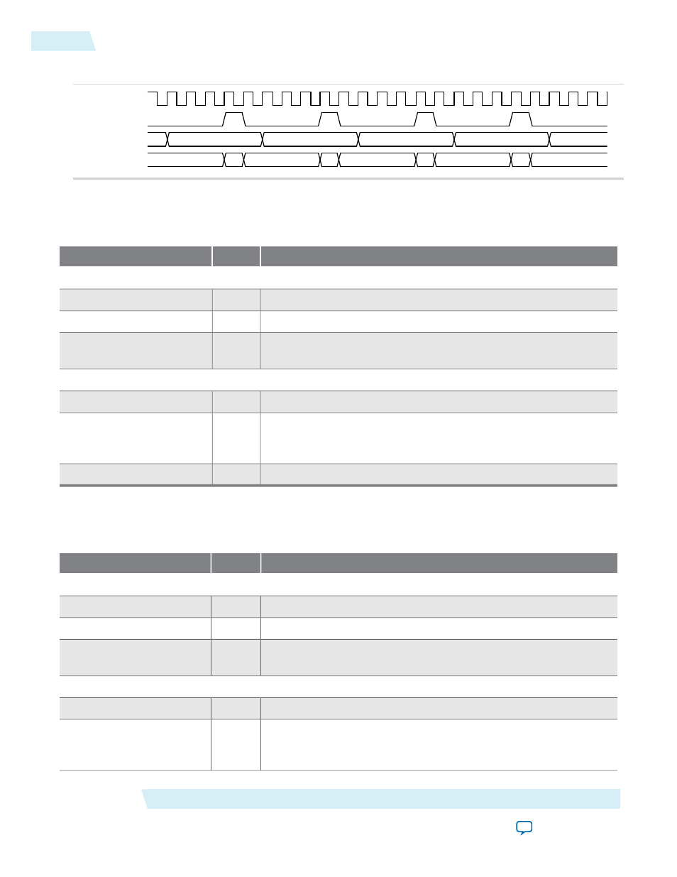
Figure 7-8: Clock Enabler Signal Behavior
125 MHz Clock
25 MHz Clock Enable
Input Data
Output Data
0xAA
0xAA
0xBB
0xBB
0xCC
0xCC
0xDD
0xDD
0xEE
GMII
Table 7-39: GMII Signals
Description
I/O
Name
GMII Transmit Interface
GMII transmit data bus.
I
gmii_tx_d[7:0]
Assert this signal to indicate that the data on
gmii_tx_d[7:0]
is valid.
I
gmii_tx_en
Assert this signal to indicate to the PHY device that the current frame
sent is invalid.
I
gmii_tx_err
GMII Receive Interface
GMII receive data bus.
O
gmii_rx_d[7:0]
Asserted to indicate that the data on
gmii_rx_d[7:0]
is valid. Stays
asserted during frame reception, from the first preamble byte until
the last byte in the CRC field is received.
O
gmii_rx_dv
Asserted by the PHY to indicate that the current frame contains errors.
O
gmii_rx_err
MII
Table 7-40: MII Signals
Description
I/O
Name
MII Transmit Interface
MII transmit data bus.
I
mii_tx_d[3:0]
Assert this signal to indicate that the data on
mii_tx_d[3:0]
is valid.
I
mii_tx_en
Assert this signal to indicate to the PHY device that the frame sent is
invalid.
I
mii_tx_err
MII Receive Interface
MII receive data bus.
O
mii_rx_d[3:0]
Asserted to indicate that the data on
mii_rx_d[3:0]
is valid. The signal
stays asserted during frame reception, from the first preamble byte
until the last byte of the CRC field is received.
O
mii_rx_dv
Interface Signals
Altera Corporation
UG-01008
GMII
7-36
2014.06.30