Datasheet, Arria 10 avalon-mm interface for pcie datasheet, Datasheet -1 – Altera Arria 10 Avalon-MM User Manual
Page 7: Arria 10 avalon-mm interface for pcie datasheet -1
Datasheet
1
2015.05.14
UG-01145_avmm
Arria 10 Avalon-MM Interface for PCIe Datasheet
Altera
®
Arria
®
10 FPGAs include a configurable, hardened protocol stack for PCI Express
®
that is
compliant with PCI Express Base Specification 3.0.
The Hard IP for PCI Express IP core using the Avalon
®
Memory-Mapped (Avalon-MM) interface
removes some of the complexities associated with the PCIe protocol. For example, it handles all of the
Transaction Layer Protocol (TLP) encoding and decoding. Consequently, you can complete your design
more quickly. The Avalon-MM interface is implemented as a bridge in soft logic. It is available in Qsys.
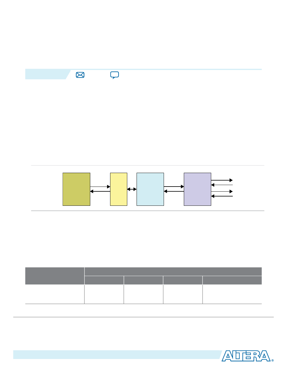
Figure 1-1: Arria 10 PCIe Variant with Avalon-MM Interface
The following figure shows the high-level modules and connecting interfaces for this variant.
Bridge
PCIe Hard IP
Block
PIPE
Interface
PHY IP Core
for PCIe
(PCS/PMA)
Serial Data
Transmission
Application
Layer
(User Logic)
Avalon-MM
Interface
Table 1-1: PCI Express Data Throughput
The following table shows the aggregate bandwidth of a PCI Express link for Gen1, Gen2, and Gen3 for 1, 2, 4,
and 8 lanes. The protocol specifies 2.5 giga-transfers per second for Gen1, 5.0 giga-transfers per second for Gen2,
and 8.0 giga-transfers per second for Gen3. This table provides bandwidths for a single transmit (TX) or receive
(RX) channel. The numbers double for duplex operation. Gen1 and Gen2 use 8B/10B encoding which introduces
a 20% overhead. In contrast, Gen3 uses 128b/130b encoding which reduces the data throughput lost to encoding
to less than 1%.
Link Width in Gigabits Per Second (Gbps)
x1
x2
x4
x8
PCI Express Gen1
(2.5 Gbps)
2
4
8
16
©
2015 Altera Corporation. All rights reserved. ALTERA, ARRIA, CYCLONE, ENPIRION, MAX, MEGACORE, NIOS, QUARTUS and STRATIX words and logos are
trademarks of Altera Corporation and registered in the U.S. Patent and Trademark Office and in other countries. All other words and logos identified as
trademarks or service marks are the property of their respective holders as described at
www.altera.com/common/legal.html
. Altera warrants performance
of its semiconductor products to current specifications in accordance with Altera's standard warranty, but reserves the right to make changes to any
products and services at any time without notice. Altera assumes no responsibility or liability arising out of the application or use of any information,
product, or service described herein except as expressly agreed to in writing by Altera. Altera customers are advised to obtain the latest version of device
specifications before relying on any published information and before placing orders for products or services.
www.altera.com
101 Innovation Drive, San Jose, CA 95134