Configuration space register access, Configuration space register access –34 – Altera Arria V Hard IP for PCI Express User Manual
Page 132
7–34
Chapter 7: IP Core Interfaces
Arria V Hard IP for PCI Express
Arria V Hard IP for PCI Express
December 2013
Altera Corporation
User Guide
Configuration Space Register Access
The
tl_cfg_ctl
signal is a multiplexed bus that contains the contents of
Configuration Space registers as shown in
Table 7–11
. Information stored in the
Configuration Space is accessed in round robin order where
tl_cfg_add
indicates
which register is being accessed.
shows the layout of configuration
information that is multiplexed on
tl_cfg_ctl
.
describes the Configuration Space registers referred to in
Table 7–11
and
.
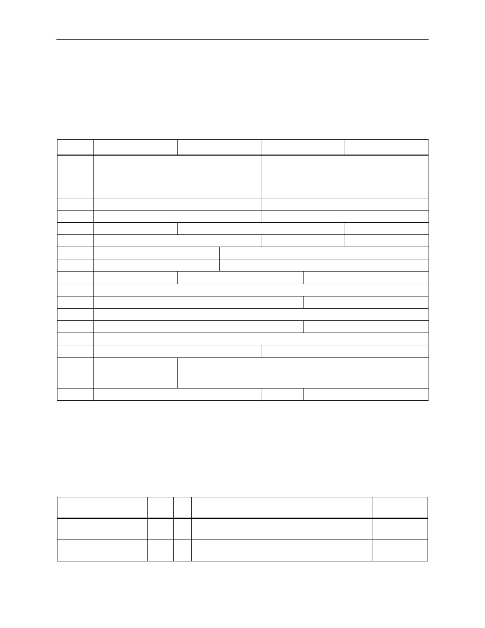
Table 7–13. Multiplexed Configuration Register Information Available on tl_cfg_ctl
Index
31:24
23:16
15:8
7:0
0
cfg_dev_ctrl_func<n>[15:0]
cfg_dev_ctrl2[15:0]
cfg_dev_ctrl[14:12]=
Max Read Req Size
cfg_dev_ctrl[7:5]=
Max Payload
1
16’h0000
cfg_slot_ctrl[15:0]
2
cfg_link_ctrl[15:0]
cfg_link_ctrl2[15:0]
3
8’h00
cfg_prm_cmd_func<n>[15:0]
cfg_root_ctrl[7:0]
4
cfg_sec_ctrl[15:0]
cfg_secbus[7:0]
cfg_subbus[7:0]
5
cfg_msi_addr[11:0]
cfg_io_bas[19:0]
6
cfg_msi_addr[43:32]
cfg_io_lim[19:0]
7
8h’00
cfg_np_bas[11:0] cfg_np_lim[11:0]
8
cfg_pr_bas[31:0]
9
cfg_msi_addr[31:12]
cfg_pr_bas[43:32]
A
cfg_pr_lim[31:0]
B
cfg_msi_addr[63:44]
cfg_pr_lim[43:32]
C
cfg_pmcsr[31:0]
D
cfg_msixcsr[15:0]
cfg_msicsr[15:0]
E
6’h00,
tx_ecrcgen[25],
rx_ecrccheck[24]
cfg_tcvcmap[23:0]
F
cfg_msi_data[15:0]
3’b000
cfg_busdev[12:0]
Notes to
:
(1) Items in
blue
are only available for Root Ports.
(2) This field is encoded as specified in Section 7.8.4 of th
. (3’b000–3’b101 correspond to 128–4096 bytes).
(3)
rx_ecrccheck
and
tx_ecrcgen
are bit s 24 and 25 of
tl_cfg_ctl
, respectively. (Other bit specifications in this table indicate the bit location
within the Configuration Space register.)
Table 7–14. Configuration Space Register Descriptions (Part 1 of 4)
Register
Width
Dir
Description
Register
Reference
cfg_dev_ctrl_func<n>
16
O
cfg_dev_ctrl_func<n>[15:0]
is Device Control
register for the PCI Express capability structure.
cfg_dev_ctrl2
16
O
cft_dev_ctrl2[31:16]
is Device Control register 2 for
the PCI Express capability structure.