0x02c, 0x05c, 0x068 – Altera Arria V Hard IP for PCI Express User Manual
Page 157: 0x06c, 0x050
Chapter 8: Register Descriptions
8–3
Configuration Space Register Content
December 2013
Altera Corporation
Arria V Hard IP for PCI Express
User Guide
describes the MSI Capability structure.
describes the MSI-X Capability structure.
0x024
Prefetchable Memory Limit
Prefetchable Memory Base
0x028
Prefetchable Base Upper 32 Bits
0x02C
Prefetchable Limit Upper 32 Bits
0x030
I/O Limit Upper 16 Bits
I/O Base Upper 16 Bits
0x034
Reserved
Capabilities
Pointer
0x038
Expansion ROM Base Address
0x03C
Bridge Control
Interrupt Pin
Interrupt Line
Note to
(1) Refer to
for a comprehensive list of correspondences between the Configuration Space regist
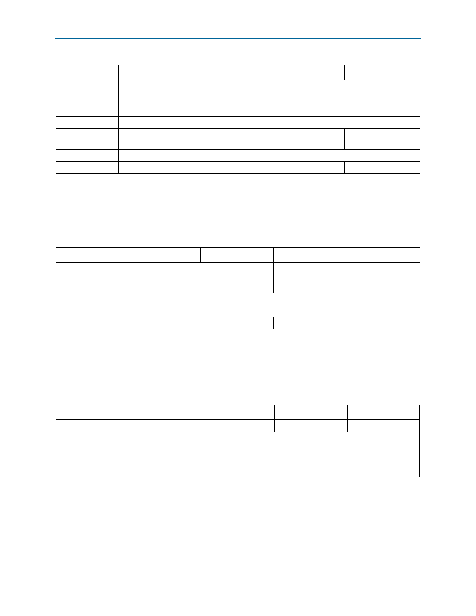
Table 8–3. PCI Type 1 Configuration Space Header (Root Ports) (Part 2 of 2)
Byte Offset
31:24
23:16
15:8
7:0
Table 8–4. MSI Capability Structure, Rev2.1 Spec: MSI Capability Structures
Byte Offsets
31:24
23:16
15:8
7:0
0x050
Message Control
Configuration MSI Control Register Field
Next Cap Ptr
Capability ID
0x054
Message Address
0x058
Message Upper Address
0x05C
Reserved
Message Data
Note to
(1) Specifies the byte offset within Arria V Hard IP for PCI Express IP core’s address space.
(2) Refer to
for a comprehensive list of correspondences between the Configuration Space regist
Table 8–5. MSI-X Capability Structure, Rev2.1 Spec: MSI-X Capability Structures
Byte Offset
31:24
23:16
15:8
7:3
2:0
0x068
Message Control
Next Cap Ptr
Capability ID
0x06C
MSI-X Table Offset
0x070
PBA Offset
Pending Bit Array (PBA) Offset
Note to
(1) Refer to
for a comprehensive list of correspondences between the Configuration Space registers and the